CMOS image sensor having photodiode and method for manufacturing the same

a technology of photodiodes and image sensors, which is applied in the field of cmos image sensors, can solve the problems of inefficiency in the manufacturing process, microlens damage, and inconvenient addition of process steps, and achieve the effect of improving the light-reflection properties of microlenses

Inactive Publication Date: 2007-10-09
DONGBU ELECTRONICS CO LTD
View PDF5 Cites 5 Cited by
  • Summary
  • Abstract
  • Description
  • Claims
  • Application Information

AI Technical Summary

Benefits of technology

[0015]The present invention provides a CMOS image sensor and a method for manufacturing the same, in which a microlens is formed between each light-shielding layer, where each light-shielding layer is formed in shape of a upside-down T, thereby improving the light-reflection properties of the microlenses and protecting the microlenses during packaging.

Problems solved by technology

However, it is inefficient in that it necessarily requires an additional process step.
Also, the microlens may be damaged during the packaging process.
When using the light-shielding layer, it is necessary to form the insulating layer for protecting the light-shielding layer, thereby causing inefficiency in the manufacturing process.
Also, since the packaging process is performed on the microlenses, the microlenses may be damaged.

Method used


Image

  • CMOS image sensor having photodiode and method for manufacturing the same
  • CMOS image sensor having photodiode and method for manufacturing the same
  • CMOS image sensor having photodiode and method for manufacturing the same

Examples


Embodiment Construction

[0029]Reference will now be made in detail to the preferred embodiments of the present invention, examples of which are illustrated in the accompanying drawings. Wherever possible, the same reference numbers will be used throughout the drawings to refer to the same or like parts.

[0030]Hereinafter, a CMOS image sensor and a method for manufacturing the same according to an exemplary embodiment the present invention will be described with reference to the accompanying drawings.

[0031]FIGS. 2A to 2F are cross sectional views of showing a CMOS image sensor manufactured according to an exemplary embodiment of the present invention.

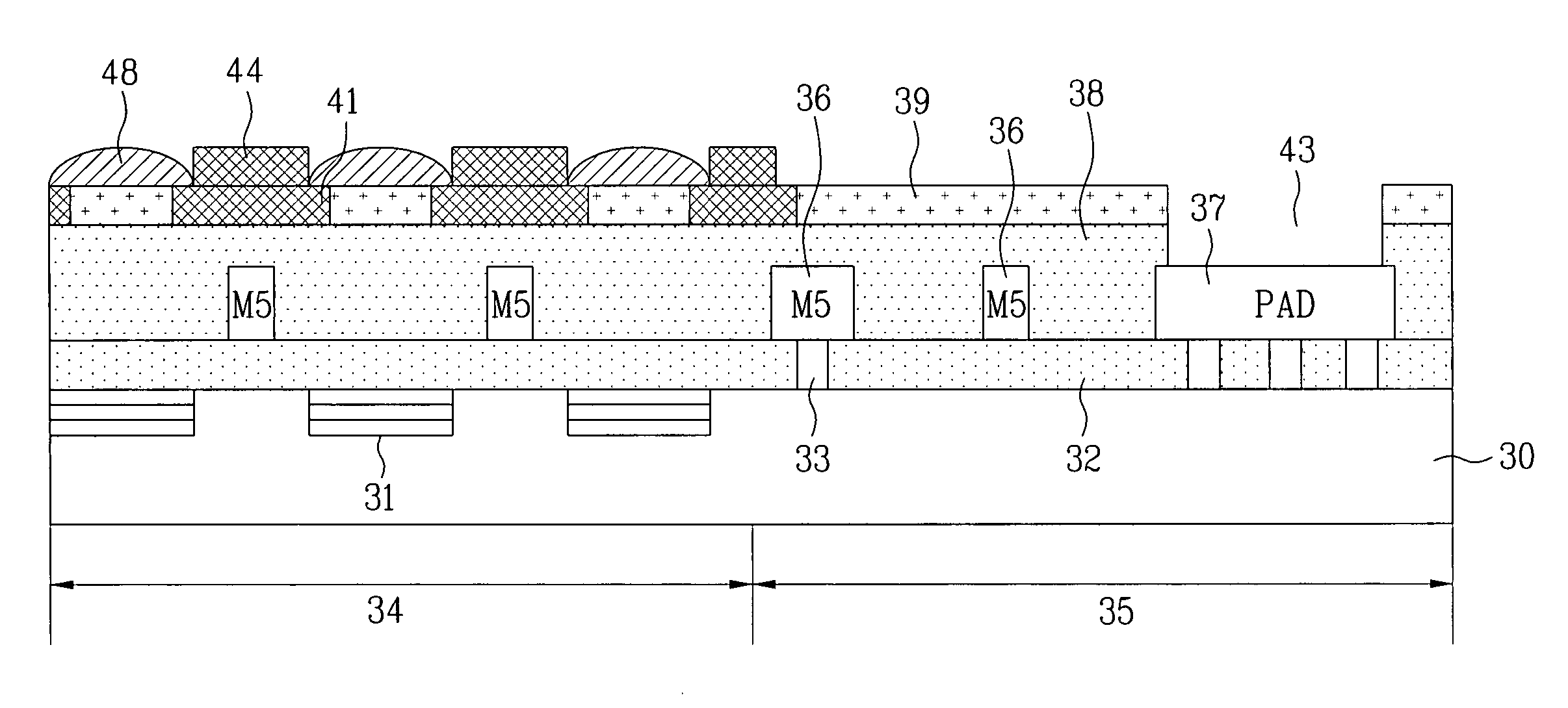
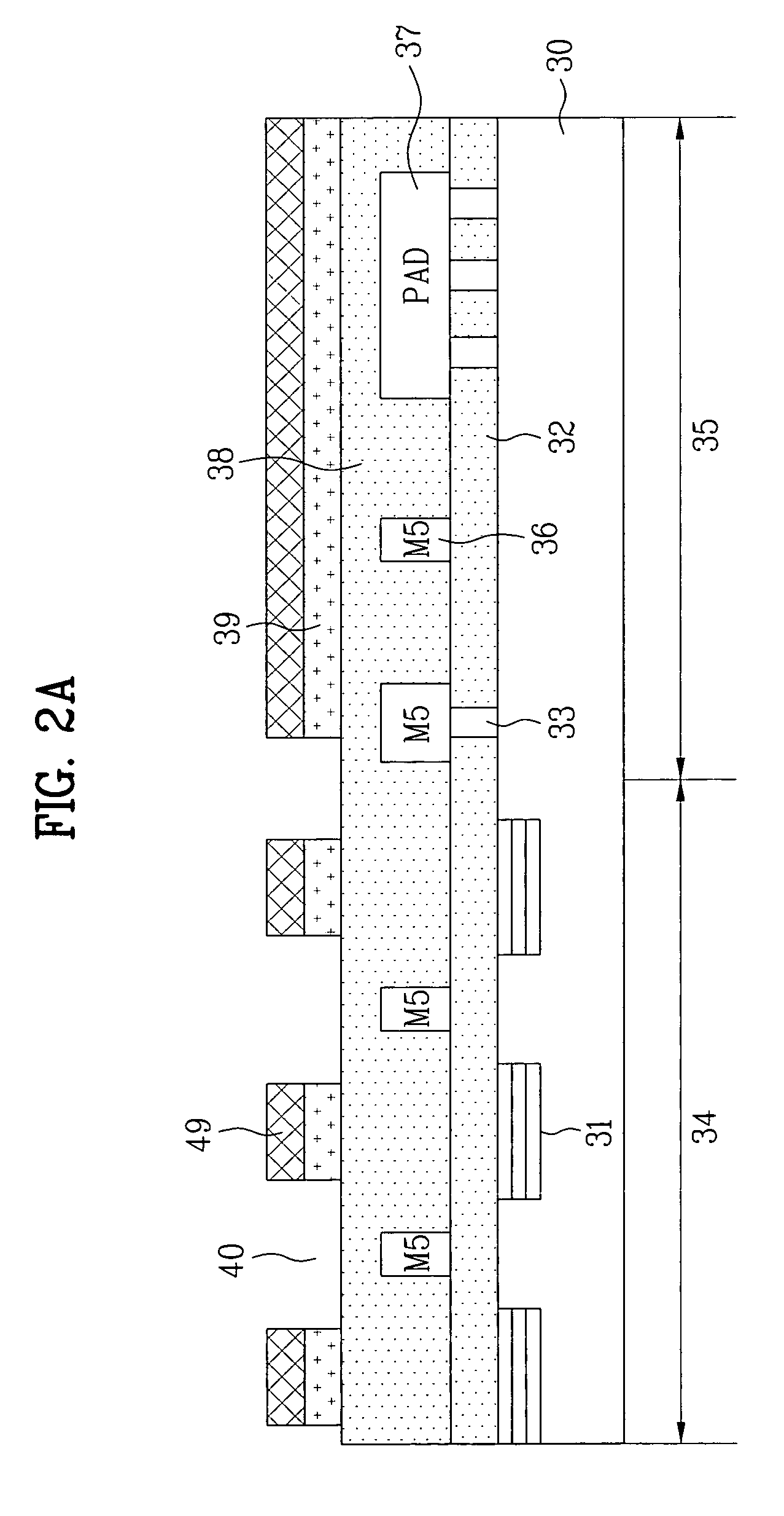
[0032]As shown in FIG. 2A, a plurality of photodiodes 31 are in a semiconductor substrate 30. Then, a first insulating layer 32 is formed on the semiconductor substrate 30, including the plurality of photodiodes 31, and is then selectively etched to form a via-hole. The via-hole is filled with a conductive material, thereby forming a contact 33.

[0033]Subsequentl...


PUM


Abstract

A CMOS image sensor includes a photodiode in a semiconductor substrate; an insulating interlayer over the semiconductor substrate including the photodiode; a passivation layer pattern on the insulating interlayer corresponding to the photodiode; a first light-shielding layer pattern on the insulating interlayer between each passivation layer pattern; a second light-shielding layer pattern on the first light-shielding layer pattern; and at least one microlens on the passivation layer pattern.

Description

CROSS-REFERENCE TO RELATED APPLICATION[0001]This application claims the benefit of Korean Patent Application No. 10-2004-0117183, filed on Dec. 30, 2004, which is hereby incorporated by reference for all purposes as if fully set forth herein.BACKGROUND OF THE INVENTION[0002]1. Field of the Invention[0003]The present invention relates to a CMOS image sensor and a method for manufacturing the same, and more particularly, to a CMOS image sensor and a method for manufacturing the same, in which a microlens is formed between each light-shielding layer formed in the shape of an upside-down T, thereby improving the light-reflection properties of the microlenses and protecting the microlenses during or within packaging.[0004]2. Discussion of the Related Art[0005]Generally, an image sensor is a semiconductor device for converting an optical image to an electric signal. The image sensor can be broadly categorized into a charge coupled device (CCD) or a complementary metal oxide semiconductor ...

Claims


Application Information

Patent Timeline
Patent Type & Authority Patents(United States)
IPC IPC(8): H01L31/0232
CPCH01L27/14623H01L27/14685H01L27/14636H01L27/14627H01L27/146H01L31/10
Inventor LEE, SANG GI
Owner DONGBU ELECTRONICS CO LTD
Why Eureka
Try Eureka