Liquid crystal device, a method for producing a liquid crystal device and a method for controlling a liquid crystal device

a liquid crystal device and liquid crystal technology, applied in the field of liquid crystal devices, can solve the problems of non-satisfactory brightness and switching times, slow display, and fast display speed

Inactive Publication Date: 2007-10-16
ECSIBEO PPF1
View PDF39 Cites 4 Cited by
  • Summary
  • Abstract
  • Description
  • Claims
  • Application Information

AI Technical Summary

Benefits of technology

[0051]The claimed invention makes it possible to induce a local variation of one or more physical properties of the liquid crystal material within a restricted volume (here termed “sub-volume” or “sub-region”) of the bulk layer adjacent to said dopant surface.
[0087]Thus, in accordance with the claimed invention, the physical properties in the surface sub-region may be effectively changed by the dopants that are permanently attached to the said dopant surface. The amplitude and / or the sign of the dielectric anisotropy as well as of the flexoelectric polarisation may be changed. The magnitude of the scalar order parameter as well as the one of the surface viscosity may be decreased and increased, respectively. As consequence, the surface sub-region will behave differently from the liquid crystal bulk under an applied electric field.
[0110]Thus, the invention makes it possible to achieve a local variation of one or more physical properties of a liquid crystal host material, like spontaneous polarisation, pitch, optical activity, dielectric anisotropy, flexoelectric polarization, scalar order parameter, viscosity, etc, which in its turn may be used for controlling the bulk layer indirectly via the doped region.

Problems solved by technology

These displays are usually slow, and nearly all suffer from non-satisfactory angular dependence of the contrast due to the switching of the liquid crystal molecules in a plane formed by the initial orientation of the molecules and the applied electric field (so-called out-of-plane switching).
These displays exhibit a very small angular dependence of the image contrast but the brightness and the switching times are not satisfactory.
However, the Ps is spiralling, thus resulting in self-cancelling of the local polarisation.
Drawbacks of the surface stabilized FLC and AFLC displays include difficulties in orienting the chiral smectic phases and maintaining their orientation.
The FLC displays in addition have a sticking image problem due to building surface charged layers.
The power consumption of these displays is also relatively high.
Yet another drawback is that the thickness of the liquid crystal layer in these devices must be of order 1-1.5 μm in order to obtain the unwound state of these materials.
This requirement for small thickness makes the production of FLC and AFLC displays complicated, delicate and very expensive.
However, in some cases the liquid crystal molecules near the solid surfaces are difficult to reorient by an electric field, due to the above-mentioned surface liquid crystal interactions, whereas the “bulk molecules” more remote from the surfaces are fairly free and therefore easy to reorient by the field.
A drawback of using photo commanded alignment surfaces in order to switch a liquid crystal alignment between two states is the low speed.
Another drawback is that the life-time of a device having a photo commanded alignment surface is reduced by the degradation processes that take place due to UV-irradiation.
Moreover, the use of light as external factor for switching the alignment of the liquid crystal is not convenient especially for liquid crystal displays.
However, as pointed out already, there are several problems related to the use of ferroelectric liquid crystals in displays and devices.

Method used


Image

  • Liquid crystal device, a method for producing a liquid crystal device and a method for controlling a liquid crystal device
  • Liquid crystal device, a method for producing a liquid crystal device and a method for controlling a liquid crystal device
  • Liquid crystal device, a method for producing a liquid crystal device and a method for controlling a liquid crystal device

Examples


example 1

Method of Preparation

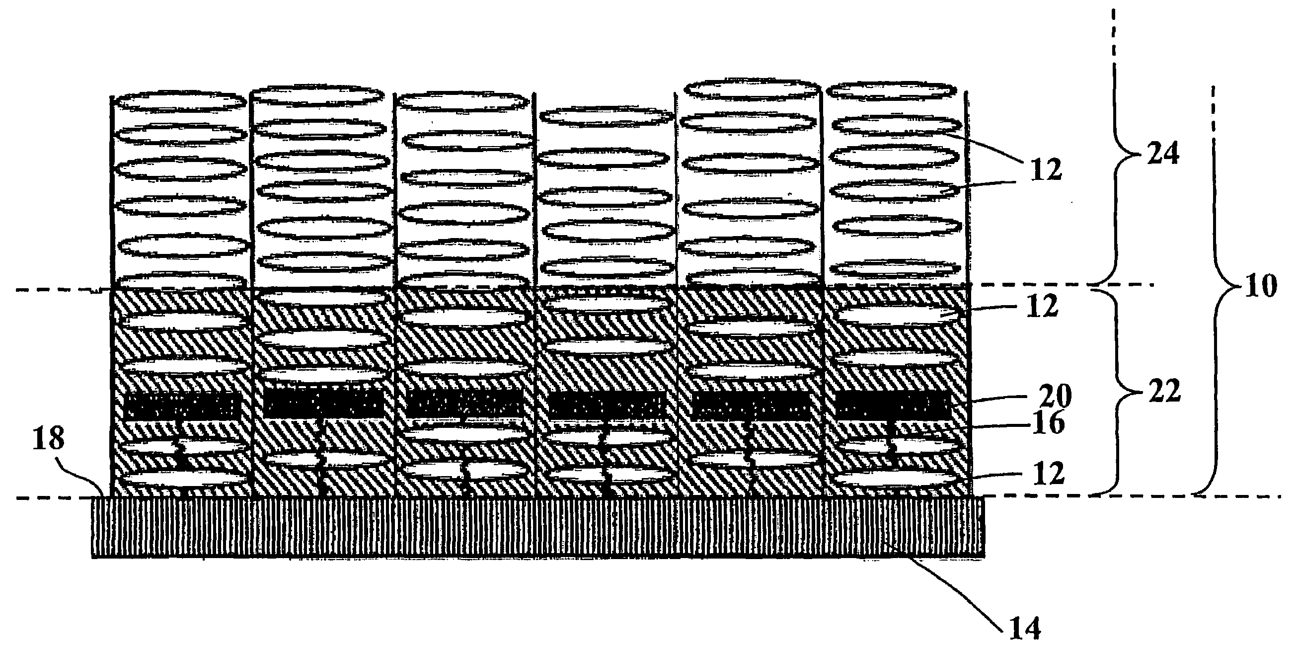
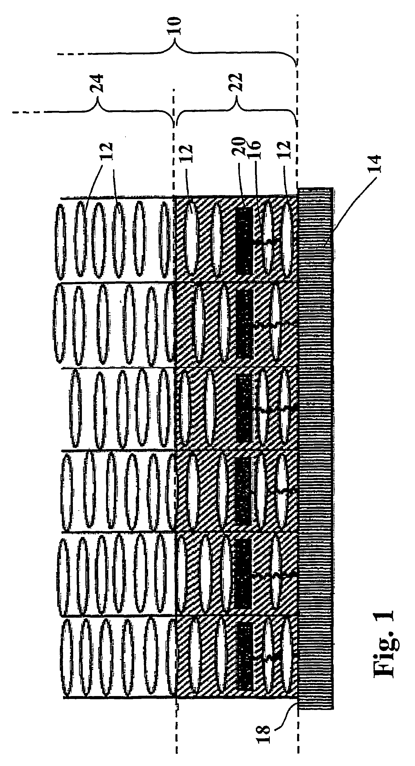
[0147]In one embodiment for the preparation of a chiral surface layer as illustrated in FIG. 3 or 4, the inner surface of the glass or plastic substrate 14 is first covered by transparent, conductive ITO film 30 and, thereafter, with an alignment layer 32 of e.g. a thin Au film, evaporated at normal incidence. The alignment layer 32 may be a passive alignment layer.

[0148]Then, the alignment layer 32 is covered by a thin film 20 comprising, in this example, a photosensitive organic material including chiral molecules 20. This chiral material 20 may be of the side-on type of attachment of chiral moieties at ortho- or meta-position anchored on to Au film through sulphur-containing group. The molecular structure of the organic chiral material 20 may be the following:

[0149]

[0150]The substrate 14, which now has been covered by the thin layer of photosensitive chiral material 20, is exposed to linearly polarised UV light in order to obtain a unidirectional planar, pred...

example 2

Method of Preparation

[0151]In a second example, the chiral surface may be prepared by a thin film of organic material containing a mixture of chiral molecules of the same kind as in the Example 1 but in this case they possess different length of the coupling group as shown schematically below:

[0152]

[0153]The length of the coupling group will define the maximum distance between the chiral dopant molecule and the surface. However, the chiral dopant molecule may be free to move in a direction towards the surface.

example 3

Method of Preparation

[0154]According to Example 3, in order to prepare a chiral surface forming e.g. the first thin film of chiral molecules 20 depicted in e.g. FIG. 4, the transparent conductive ITO film 30 of the glass substrate 14 is covered by a passive alignment layer 32 of buffed SiOx film, evaporated at normal incidence, for instance. As well known, this passive alignment layer gives unidirectional planar alignment of most liquid crystal materials. The same kind of alignment could be obtained by evaporating the SiOx film 32 at angle of incidence α˜60° with respect to the substrate surface 18. Thereafter, the passive alignment layer 32 is covered by a thin film of photosensitive organic chiral material 20 of the kind described in example 1. The molecules of this material may be permanently attached to the silica surface by the use of e.g. silylation.


PUM

PropertyMeasurementUnit
thicknessaaaaaaaaaa
electric fieldaaaaaaaaaa
molecular tilt angleaaaaaaaaaa

Abstract

The invention relates to a liquid crystal device, comprising a liquid crystal bulk layer and dopants being inhomogeneously distributed in the bulk layer as a result of being permanently attached to at least one surface, termed dopant surface. The invention also relates to methods for manufacturing as well as methods for controlling liquid crystal devices.

Description

TECHNICAL FIELD[0001]The present invention is related to the field of liquid crystals. More specifically, it is related to a liquid crystal device including a liquid crystal bulk layer and dopants dissolved in this layer in an inhomogeneous distribution manner. The invention also relates to a method for producing a liquid crystal device including dopants inhomogeneously distributed in the liquid crystal bulk layer. The invention also relates to a method of controlling a liquid crystal device.TECHNICAL BACKGROUND[0002]Liquid crystals, widely used at present as electro-optical media in display devices, are organic materials with anisotropic physical properties. The operation of the liquid crystal displays is based on the changes of the optical appearance of the liquid crystal in the display caused by an applied electric field.[0003]One of the basic operational principle of liquid crystal displays and devices is the switching of the orientation of the liquid crystal molecules by an app...

Claims


Application Information

Patent Timeline
Patent Type & Authority Patents(United States)
IPC IPC(8): G02F1/1337C09K19/02G02F1/139C09K19/40C09K19/58G02F1/141
CPCC09K19/02C09K19/0225C09K19/0266C09K19/408G02F1/133703C09K19/586G02F2001/133769C09K2019/0418G02F2001/133726G02F1/133726G02F1/133769G02F1/137G02F1/141
Inventor HELGEE, BERTILKOMITOV, LATCHEZAR
Owner ECSIBEO PPF1
Why Eureka
Try Eureka