Curved grating spectrometer with very high wavelength resolution

a spectrometer and curved grating technology, applied in the field of semiconductor photonic and optoelectronic devices, can solve the problems of limiting wavelength resolution, reducing the resolution of refocusing beams, and limiting wavelength resolution, so as to achieve small rs factors, and reduce the cost of production.

Active Publication Date: 2007-10-16
PHOSISTOR TECH
View PDF4 Cites 27 Cited by
  • Summary
  • Abstract
  • Description
  • Claims
  • Application Information

AI Technical Summary

Benefits of technology

[0021]It is an aim of the invention to provide a compact curved grating and associated compact curved grating spectrometer that is capable of achieving very small RS factors thereby enabling high resolution at small size.

Problems solved by technology

This is primarily because of the various limitations in the current art (as will be described below).
Aberration limitation: In the case of the Rowland design, when θdiv>4DEG, serous aberration in the refocusing beam will occur to limit wavelength resolution.
In short, the current designs are close to their resolution-size (RS) limits and cannot be made substantially more compact without losing wavelength resolution.
The challenge is to circumvent the current limitation in grating spectrometer design and fabrication methods.
While several current technologies are capable of using planar waveguide technologies to make grating based spectrometers on a single silica or semiconductor substrate, they are still not able to achieve RS much smaller than 10 due to the basic limitations of the grating spectrometer design.
The costs of these integrated WDM devices are typically proportional to their sizes.

Method used


Image

  • Curved grating spectrometer with very high wavelength resolution
  • Curved grating spectrometer with very high wavelength resolution
  • Curved grating spectrometer with very high wavelength resolution

Examples


Embodiment Construction

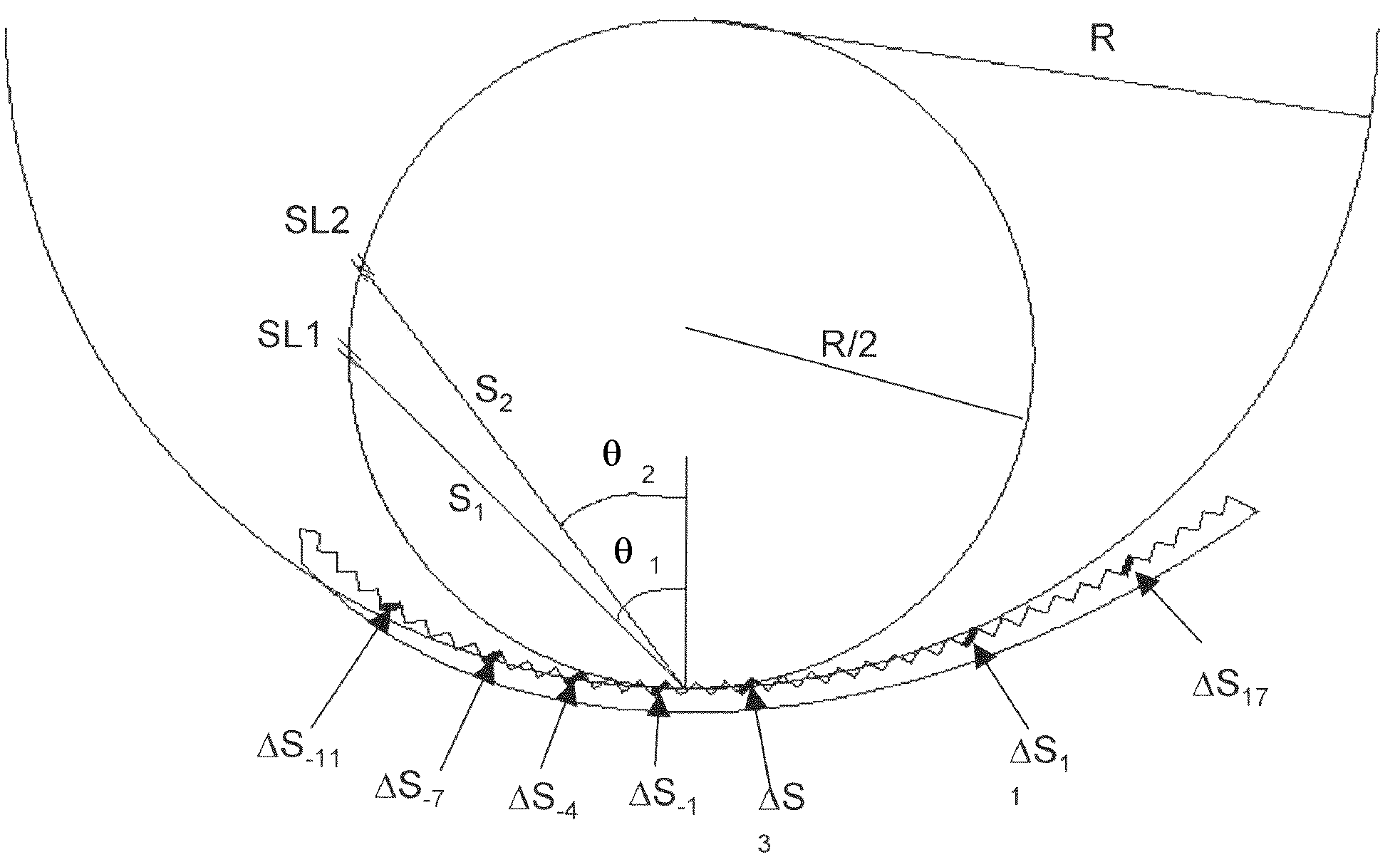
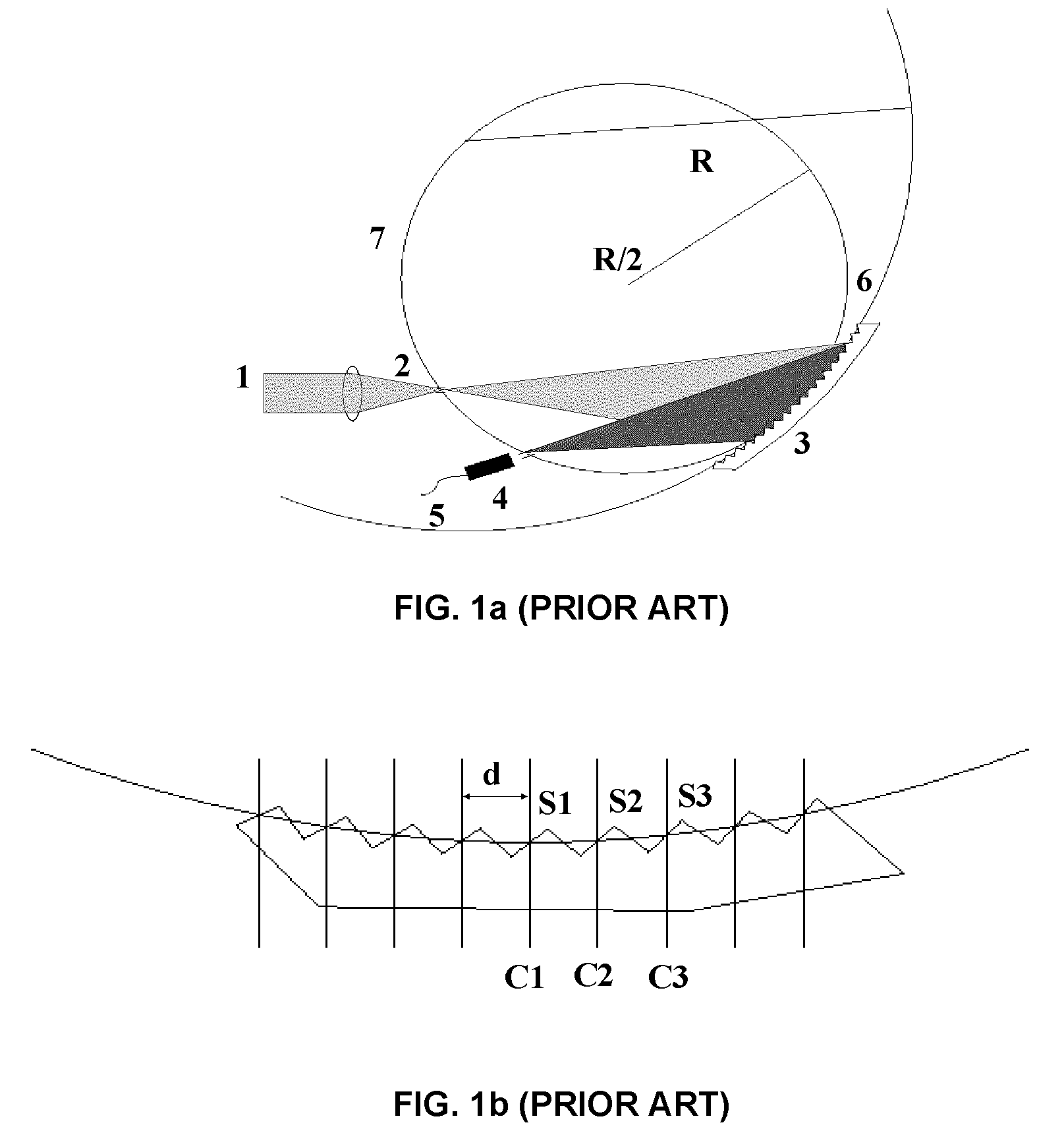
[0034]The present invention discloses a system comprising a compact curved grating (CCG), its associated compact curved grating spectrometer (CCGS) module and a method for making the same. The system is capable of achieving very small (resolution vs. size) RS factor. The uses of CCGS module include an isolated optical spectrometer using discrete optical components such as slits, grating, spectrometer casing, detector, detector array, and motor drive. More generally, the CCGS module could also be used as a wavelength dispersion element in a photonic integrated circuit. The photonic integrated circuit can be based on either of glass (silica) waveguide, semiconductor waveguide (including but not limited to, polymer waveguide, or any other type of optical waveguiding devices. Semiconductor waveguides include silicon or compound semiconductor waveguides such as III-V (GaAs, InP etc). The wavelength dispersion element based on the CCGS module in the photonic integrated circuit can be inte...


PUM


Abstract

The present invention discloses a system comprising a compact curved grating (CCG) and its associated compact curved grating spectrometer (CCGS) module and a method for making the same. The system is capable of achieving very small (resolution vs. size) RS factor. In the invention, the location of entrance slit and detector can be adjusted in order to have the best performance for a particular design goal. The initial groove spacing is calculated using a prescribed formula dependent on operation wavelength. The location of the grooves is calculated based on two conditions: the first one being that the path-difference between adjacent grooves should be an integral multiple of the wavelength in the medium and the second one being specific for a particular design goal of a curved-grating spectrometer. In an embodiment, elliptical mirrors each with focal points at the slit and detector are used for each groove to obtain aberration-free curved mirrors.

Description

CROSS REFERENCE TO RELATED APPLICATIONS[0001]This application is related to U.S. patent application Ser. No. 09 / 916,701, “Method for shifting the bandgap energy of quantum well layer” filed Jul. 26, 2001, in the names of Boon-Siew Ooi and Seng-Tiong Ho, the disclosure of which is incorporated herein by reference. This application is related to U.S. Patent Application Ser. No. 60 / 242,219, “Method for shifting the bandgap energy of quantum well layer” filed Oct. 20, 2000, in the names of Boon-Siew Ooi and Seng-Tiong Ho, the disclosure of which is incorporated herein by reference. This application is related to U.S. Patent Application Ser. No. 60 / 430,507, “Method for quantum-well intermixing using pre-annealing enhanced defect diffusion” filed Dec. 3, 2002, in the names of Boon-Siew Ooi and Ruiyu (Jane) Wang, the disclosure of which is incorporated herein by reference.BACKGROUND OF INVENTION[0002]The present invention relates to semiconductor photonic and opto-electronic devices. In pa...

Claims


Application Information

Patent Timeline
Patent Type & Authority Patents(United States)
IPC IPC(8): G01J3/28
CPCG01J3/22G01J3/20
Inventor HO, SENG-TIONGCHANG, SEONGSIK
Owner PHOSISTOR TECH
Why Eureka
Try Eureka