Vertical field-effect transistor, method of manufacturing the same, and display device having the same

a technology of vertical field and transistor, which is applied in the field of field-effect transistors and display devices having the same, can solve the problems of destroying the value of organic electronic engineering, deteriorating the quality of a desired electric field and of the transistor structure, and the method may have a higher cost, so as to achieve excellent reproducibility and a manufacturing method. , the effect of low cos

Active Publication Date: 2007-10-23
SAMSUNG DISPLAY CO LTD
View PDF10 Cites 2 Cited by
  • Summary
  • Abstract
  • Description
  • Claims
  • Application Information

AI Technical Summary

Benefits of technology

[0015]The present invention provides, inter alia, a vertical organic field-effect transistor having excellent reproducibility and low manufacture cost, a method of manufacturing the same, and a display device having the same. More specifically, the present invention provides a vertical organic field-effect transistor that may be manufactured without using a photolithography or a shadow mask.
[0017]The present invention may provide a vertical organic field-effect transistor having an excellent reproducibility and a method for manufacturing the same. The present invention may provide a vertical organic field-effect transistor at a low cost by avoiding the use of photolithography or a shadow mask.
[0018]The present invention may provide a vertical organic field-effect transistor having excellent performance by preventing or reducing a current leakage between gate electrodes and a source electrode. This may be accomplished by arranging an insulating layer between the electrodes. The present invention may provide a display device having a vertical field-effect transistor having excellent reproducibility and low manufacture cost.

Problems solved by technology

Such migration may deteriorate the quality of a desired electric field and of the transistor structure.
Such a method may have a higher cost and may destroy the value of the organic electronic engineering.
When the gate electrode is continuously arranged to the organic material, the flow of charge carriers from the source electrode to the drain electrode may be disrupted.
More specifically, a large leakage current from the gate electrode to the source electrode may destroy the value of a field-effect transistor that can be controlled without using an electric power.

Method used


Image

  • Vertical field-effect transistor, method of manufacturing the same, and display device having the same
  • Vertical field-effect transistor, method of manufacturing the same, and display device having the same
  • Vertical field-effect transistor, method of manufacturing the same, and display device having the same

Examples


first embodiment

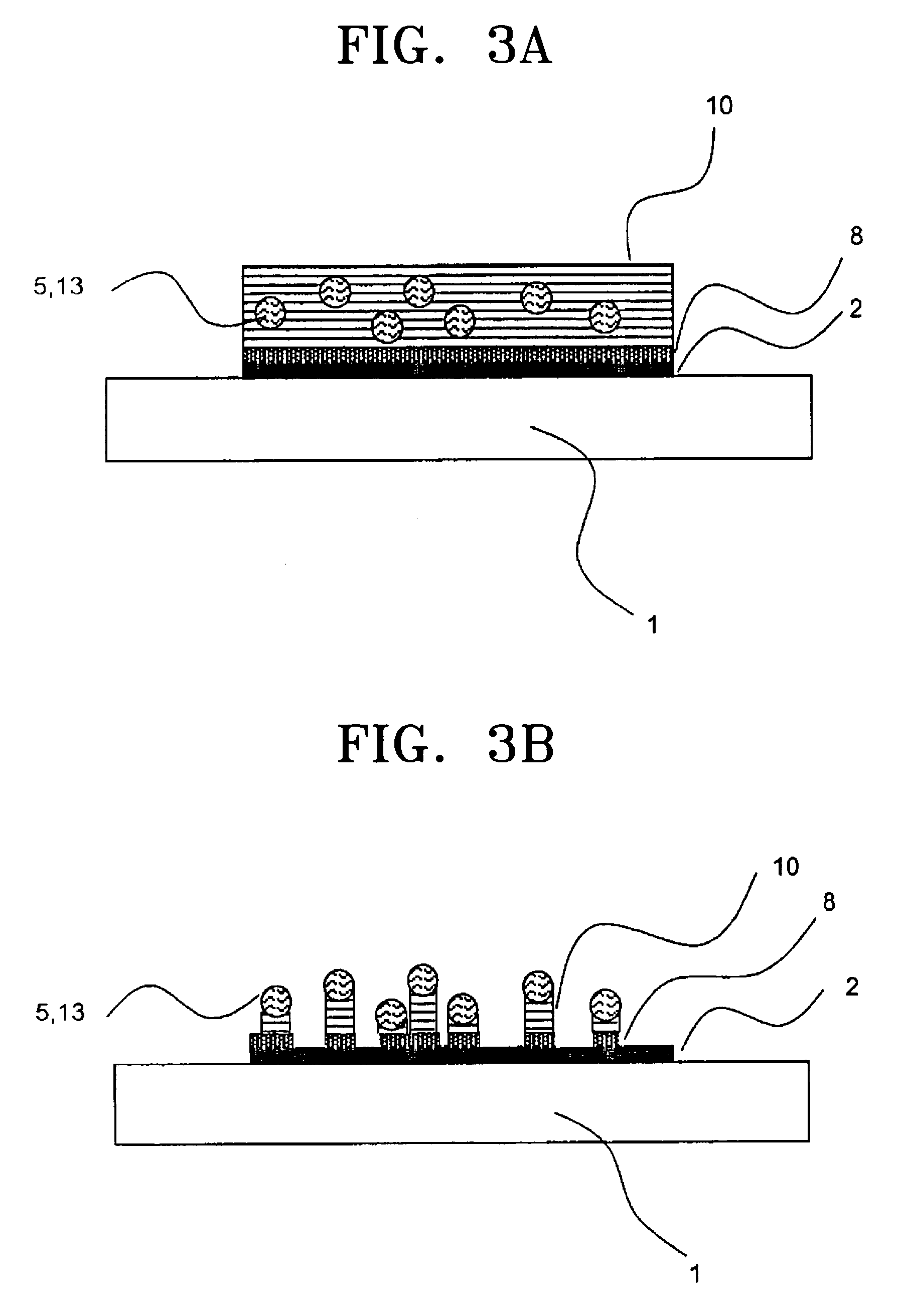
[0031]The vertical organic field-effect transistor according to the present invention may be manufactured by an anisotropic etching. The etching may selectively remove the dielectric matrix 10 and the insulating layer 8 arranged under the dielectric matrix 10 but may not damage the source electrode 2 and the gate electrodes 5. When the dielectric matrix 10 is SiOx, the etching may be performed by using, for example, an etching gas including fluorine, such as CF4, CF3H, C4F9, C2F6, CF6, or NF3.

[0032]As shown in FIG. 3C, a charge carrier block layer 4 (for example, a dielectric layer) may be formed on the gate electrodes 5 by an oxidation process such as thermal oxidation, plasma oxidation, or anodizing. Then, an organic semiconductor 3 may be deposited by vaporization under a high vacuum or spin coating from a solution. The vertical organic field-effect transistor according to the first embodiment of the present invention may be completed by applying a drain contact 6 by vaporization...

second embodiment

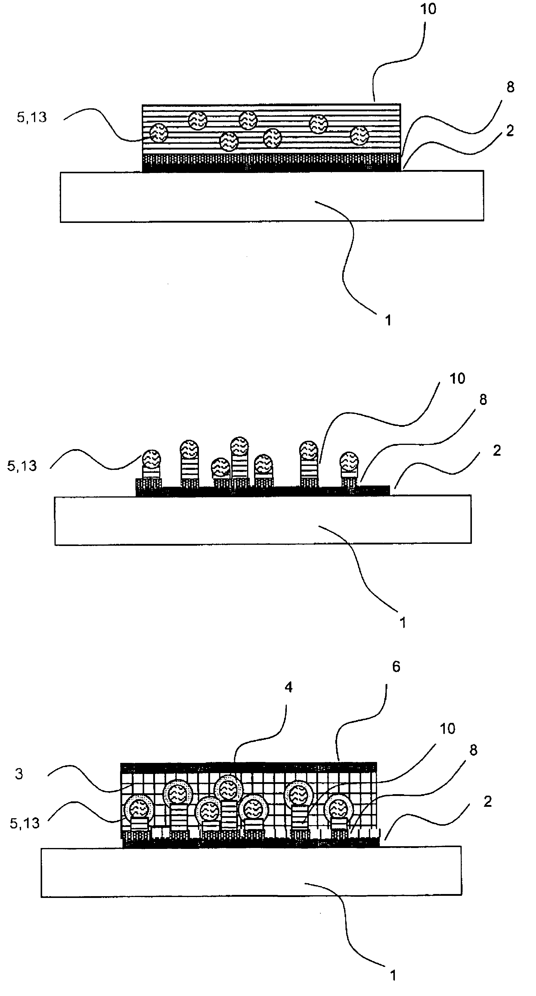
[0034]As shown in FIGS. 4A, 4B, 4C, 4D, 4E, and 4F are sectional views illustrating a method of manufacturing a vertical organic field-effect transistor according to the present invention.

[0035]A source electrode 2, an insulating layer 8, and a continuous gate electrode 5 may be deposited on a substrate. The source electrode 2 may be formed of a precious metal, such as Au, Pd, Pt, or Ni, and the insulating layer 8 may be formed of a material such as Al2O3, SiO2, SiOx, Si3Nx, TiO2, Ta2O5, ZrO2, or HfO2. The material of the gate electrode 5 may be determined based on the material of the insulating layer 8 (which may function as a dielectric layer). The gate electrode 5 and the insulating layer 8 may be formed of, for example, Al and Al2O3 or Ta and Ta2O5 in order to deposit a metal or a metal oxide without changing a target while performing sputtering.

[0036]Nanoparticles 13 to operate as an etch mask are coated on the surface of the gate electrode 5. Here, the nanoparticles 13 may be ...

third embodiment

[0039]FIGS. 5A through 5D are sectional views illustrating a method of manufacturing a vertical organic field-effect transistor according to the present invention.

[0040]In order to form a vertical organic field-effect transistor shown in FIG. 5D, the structure shown in FIG. 5A is formed. Here, a source electrode 2, an insulating layer 8, and a continuous gate electrode 5 are formed on a substrate 1. The source electrode 2 is formed of a precious metal, such as Au, Pd, Pt, and Ni, and the insulating layer 8 may be formed of Al2O3, SiO2, SiOx, TiO2, Ta2O5, ZrO2, or HfO2. The material of the gate electrode 5 is determined based on the material of the insulating layer 8. Here, the gate electrode 5 and the insulating layer 8 may be formed of Al and Al2O3 or Ta and Ta2O5.

[0041]The structure of FIG. 5A is scratched / polished by using the suspension of nanoparticles 13 having a uniform size to form grooves in the insulating layer 8 and the gate electrodes 5, as shown in FIG. 5B. Here, the na...


PUM


Abstract

Provided are a vertical field-effect transistor, a method of manufacturing the same, and a display device having the same. The method is highly reproducible and can be used to manufacture a vertical organic field-effect transistor at a low cost. In addition, the method does not require photolithography and a shadow mask. In the vertical field-effect transistor, a source electrode is formed on a substrate, and an insulating layer and discontinuous gate electrodes are formed. Then, a charge carrier block layer, an organic semiconductor material, and a drain electrode are formed. The gate electrodes are formed using nanoparticles.

Description

[0001]This application claims priority to European Patent Application No. EP 040901027, filed on Mar. 11, 2004, and Korean Patent Application No. 2004-52917, filed on Jul. 8, 2004, which are both incorporated herein in their entirety by reference.BACKGROUND OF THE INVENTION[0002]1. Field of the Invention[0003]The present invention may relate to a field-effect transistor, a display device having the same, and a method of manufacturing the same. More particularly it may relate to a vertical field-effect transistor, a display device having the same, and a method of manufacturing the same.[0004]2. Description of the Related Art[0005]Organic electronic engineering may be applied to a display device, such as an organic light emitting diode, and to a field-effect transistor. Organic electronic engineering also may realize a single electronic circuit that can be manufactured without a complicated semiconductor manufacturing process. The circuits manufactured by a method based on an organic ...

Claims


Application Information

Patent Timeline
Patent Type & Authority Patents(United States)
IPC IPC(8): H01L35/24H01L29/04G09F9/30H01L51/50H01L21/00H01L21/28H01L21/335H01L21/8238H01L21/84H01L29/06H01L29/423H01L29/49H01L29/772H01L29/786H01L29/80H01L51/00H01L51/05H01L51/40H05B33/14
CPCG09F9/30H05B33/14H01L21/28H01L21/84H01L21/00H01L29/423H01L29/49H01L29/772H01L29/786H01L51/00H01L29/80H01L51/05H01L51/50H01L29/06H01L21/8238H01L51/057H10K99/00H10K10/00H10K10/491H10K50/00B82Y10/00
Inventor REDECKER, MICHAELFISCHER, JOERGMATHEA, ARTHUR
Owner SAMSUNG DISPLAY CO LTD
Why Eureka
Try Eureka