Semiconductor integrated circuit for communication including analog-to-digital conversion circuit

a technology of analog-to-digital conversion and integrated circuit, which is applied in the direction of code conversion, transmission system, instruments, etc., can solve the problems of corresponding increase in chip cost, achieve high-precision a/d conversion, facilitate avoiding increase in the number of external terminals and the chip size, and generate reference voltages to be.

Inactive Publication Date: 2007-10-23
RENESAS ELECTRONICS CORP
View PDF6 Cites 25 Cited by
  • Summary
  • Abstract
  • Description
  • Claims
  • Application Information

AI Technical Summary

Benefits of technology

[0014]An A / D conversion circuit, if desired to achieve an A / D conversion accuracy of 10 bits or more, will require a large capacity of around a few μF, which is too large to be easily built into a semiconductor chip. It was further found out that a ΣΔ A / D conversion circuit would need at least two, or a switched capacitor type would need three, reference voltages, which means the need for three stabilization capacitors correspondingly. The number of external terminals to which the stabilization capacitors are to be connected should also be greater, inviting an increase in the number of component items required.
[0032]The invention further makes it possible to obtain a semiconductor integrated circuit with a built-in A / D conversion circuit capable of highly accurate A / D conversion while restraining the increase in the chip size, and at the same time to achieve a reduction in the size of the system using a semiconductor integrated circuit with a built-in A / D conversion circuit.

Problems solved by technology

In this case, since the baseband LSI, in spite of being mostly a digital circuit, has the A / D converter and the D / A converter, which are analog circuits, built into it, the LSI manufacturing process involves steps of forming elements to constitute the analog circuits, inviting a disadvantage that the chip cost correspondingly rises.

Method used


Image

  • Semiconductor integrated circuit for communication including analog-to-digital conversion circuit
  • Semiconductor integrated circuit for communication including analog-to-digital conversion circuit
  • Semiconductor integrated circuit for communication including analog-to-digital conversion circuit

Examples


second embodiment

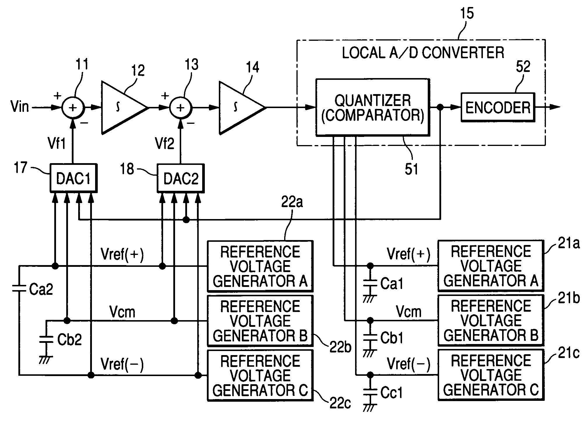
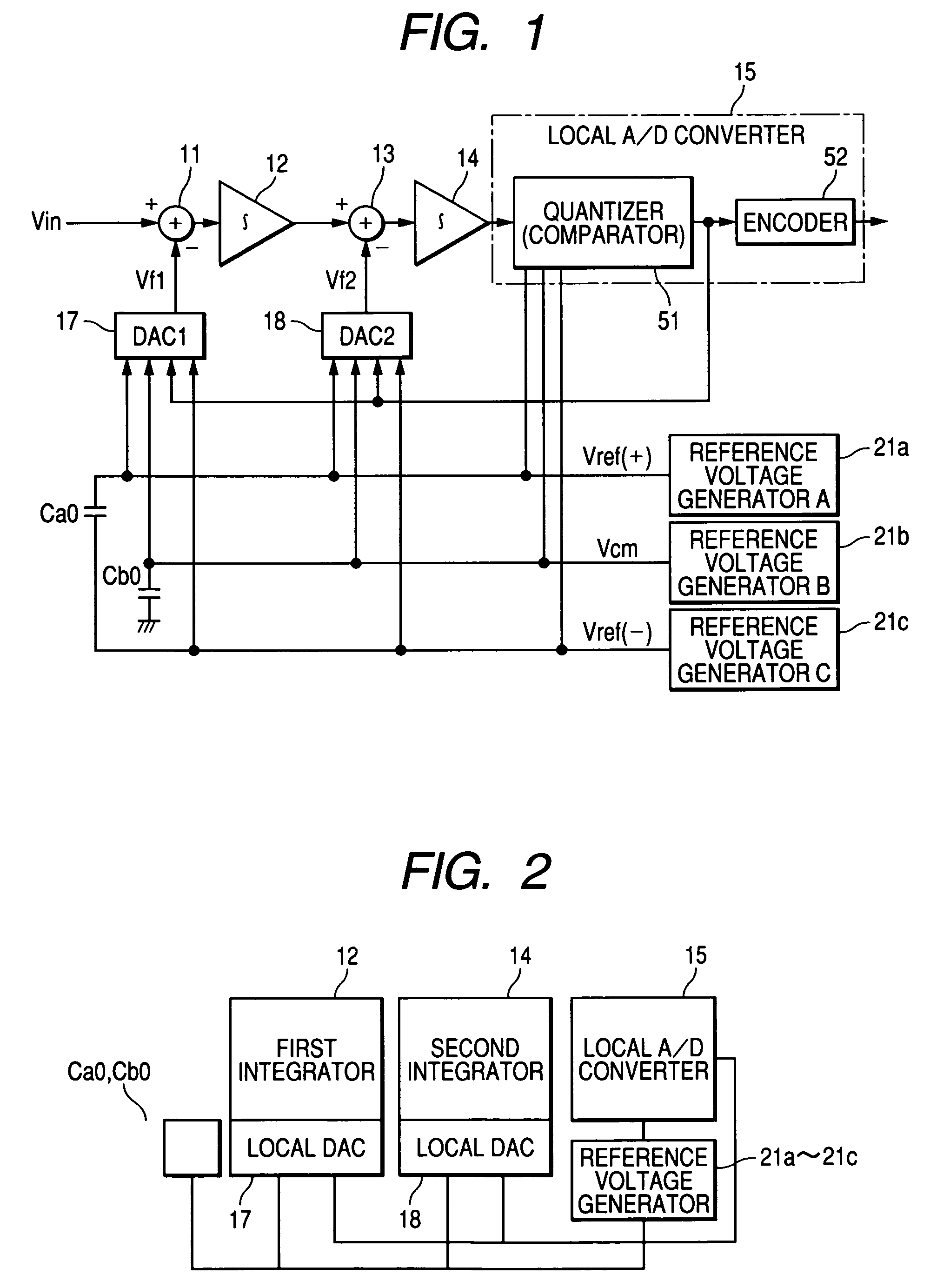
[0071]FIG. 7 shows an A / D conversion circuit, which is the invention. This embodiment, too, is an A / D conversion circuit of a second-order ΣΔ modulation system like the A / D conversion circuit shown in FIG. 1.

[0072]In this embodiment, reference voltage generators 21a, 21b and 21c for generating reference voltages Vref(+), Vcm and Vref(−) required by the local A / D converter 15 and reference voltage generators 22a, 22b, 22c for generating reference voltages Vref(+), Vcm and Vref(−) required by the local D / A converters 17 and 18 are provided as separate circuits. Along with this, reference voltage generators for generating reference voltages Vref(+), Vcm and Vref(−) required by the local D / A converters 17 and 18 are provided as reference voltage generators 22a, 22b and 22c to be used in common by the local D / A converters 17 and 18.

first embodiment

[0073]Further in this embodiment, stabilization capacitors Ca1, Cb1 and Cc1 of relatively small capacitances are provided between the output terminals and the grounding points of the reference voltage generators 21a, 21b and 21c, respectively. A stabilization capacitor Ca2 of a relatively large capacitance is provided between the output terminals of the reference voltage generators 22a and 22c, and a stabilization capacitor Cb2 of a smaller capacitance than that of Ca2 is provided between the output terminal and the grounding point of the reference voltage generator 22b. Incidentally, the capacitances of the stabilization capacitors Ca2 and Cb2 can be smaller than those of the stabilization capacitors Ca0 and Cb0 of the

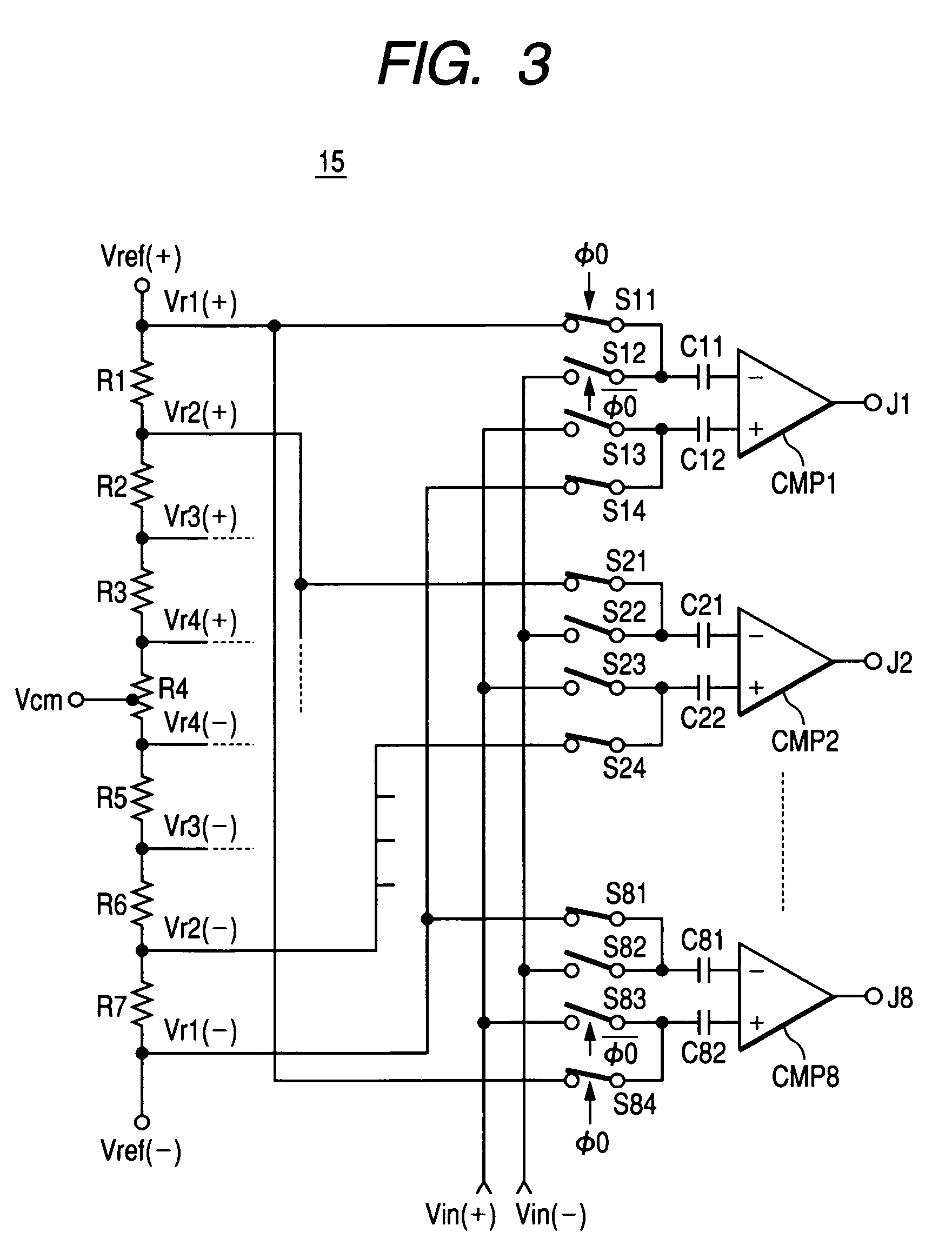
[0074]In the ΣΔ A / D conversion circuit, if the output requires an accuracy of 14 bits, while the local D / A converter will require an accuracy of 14 bits, an accuracy of 3 bits will be sufficient for the local A / D converter 15 if its output is 3 bits. Therefore, far le...


PUM


Abstract

A semiconductor integrated circuit having a built-in A / D conversion circuit which enables, where the A / D conversion circuit is to be built into a semiconductor chip, the required capacitance of the stabilization capacitor to be connected to the output terminals of reference voltage generators for generating reference voltages to be reduced is to be provided to contribute to preventing the number of external terminals and the chip size from increasing. A semiconductor integrated circuit having a built-in differential type A / D conversion circuit comprising a differential amplifier, a local A / D converter and local D / A converters, further provided with a first reference voltage generator for generating a first reference voltage and a second reference voltage generator for generating a second reference voltage both for use by the local A / D converter, wherein the first reference voltage generator and the second reference voltage generator are provided as common reference voltage generators with a reference voltage generator for generating a first reference voltage and a second reference voltage both for use by the local D / A converters, and a capacitance element for stabilizing the generated reference voltages is connected between the output terminal of the first reference voltage generator and that of the second reference voltage generator.

Description

[0001]The present application claims priority from Japanese patent application No. 2004-219830 filed on Jul. 28, 2004, the content of which is hereby incorporated by reference into this application.BACKGROUND OF THE INVENTION[0002]The present invention relates to a technique of stabilizing reference voltages for use in analog-to-digital (A / D) conversion in A / D converters for converting analog signals into digital signals and in on-chip A / D converters equipped with local A / D converters and local D / A converters, and more particularly to a technique that can be effectively used in, for instance, ΣΔ (sigma delta) type A / D converters and semiconductor integrated circuits with such converters built into them.[0003]A wireless communication system, such as a cellular phone, usually comprises a semiconductor integrated circuit (RF-IC) having functions to modulate transmit signals and to demodulate receive signals, another semiconductor integrated circuit, such as a baseband circuit for conve...

Claims


Application Information

Patent Timeline
Patent Type & Authority Patents(United States)
IPC IPC(8): H03M1/34
CPCH03M3/368H03M1/0845H03M1/365H03M1/804H03M3/454H03M1/44
Inventor KUDOH, JUNYAYAHAGI, KOUICHIMATSUURA, TATSUJI
Owner RENESAS ELECTRONICS CORP
Why Eureka
Try Eureka