System for imaging an extended area

Active Publication Date: 2007-10-23
APPL MATERIALS ISRAEL LTD
View PDF11 Cites 26 Cited by
  • Summary
  • Abstract
  • Description
  • Claims
  • Application Information

AI Technical Summary

Benefits of technology

[0006]Spiral scanning patterns have been found to be advantageous for high-speed wafer inspection, because they can be implemented simply and compactly, without the use of moving parts in the optical system. The spiral scan is better-suited for covering the surface of a circular wafer than a conventional X-Y

Problems solved by technology

Spiral scan systems known in the art, however, such as those described in the Background of the Invention, are limited to scanning the wafer surface one pixel at a time, along a single, very long spiral sca

Method used


Image

  • System for imaging an extended area
  • System for imaging an extended area

Examples


Example

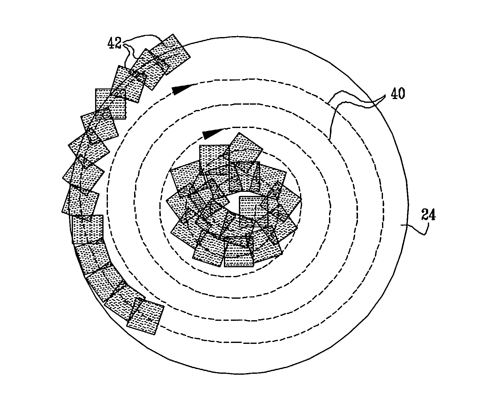
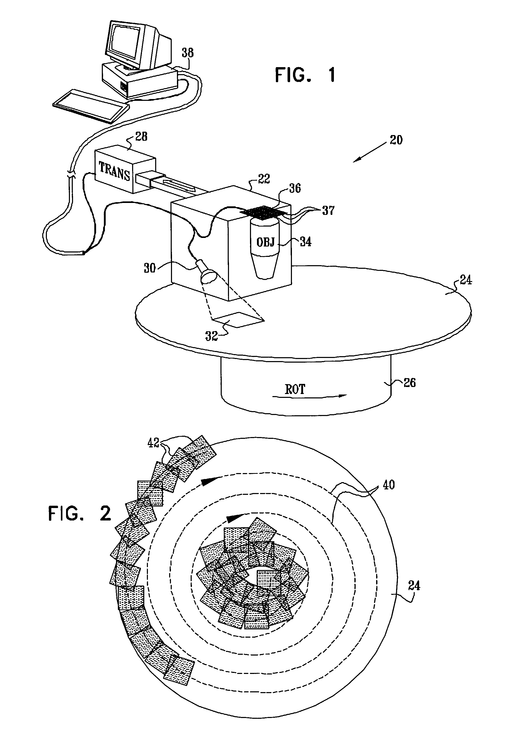
[0012]FIG. 1 is a schematic, pictorial illustration of a system 20 for optical inspection of a semiconductor wafer 24, in accordance with a preferred embodiment of the present invention. The wafer may be either unpatterned or patterned, in substantially any stage of its manufacturing process. An optical head 22, scanning on a spiral path, is used to capture a sequence of area images of the wafer surface, as described in detail hereinbelow.

[0013]Wafer 24 is preferably held by a rotating chuck 26, as is known in the art, or by another suitable rotation device. A translation device 28 translates optical head 22 over the wafer surface in a direction perpendicular to the rotation axis of the chuck. The rotation of wafer 24 and translation of head 22 are such as to enable the optical head to scan the entire wafer surface in a spiral pattern. Alternatively, the translational motion may be applied to the wafer, rather than to the optical head. Rotational motion may also be applied to the op...


PUM


Abstract

A method for optical inspection and an apparatus for optical inspection of a surface of a substrate, the apparatus includes (i) An optical head comprising a two-dimensional matrix of photodetectors, which is positioned opposite the substrate so as to capture a sequence of area images of respective areas of the surface, (ii) A rotation device, which is coupled to rotate the substrate about a rotation axis, (iii) A translation device, coupled to impart motion to at least one of the optical head and the rotation device so that the optical head is translated radially relative to the substrate while the rotation device rotates the substrate, whereby the area images in the sequence are arrayed in a spiral pattern with respect to the surface, and (iv) An image processor, which is coupled to receive and process the area images so as to determine a characteristic of the surface.

Description

FIELD OF THE INVENTION[0001]The present invention relates generally to systems and methods for optical inspection, and specifically to systems for detecting and classifying defects on substrates such as semiconductor wafers.BACKGROUND OF THE INVENTION[0002]Optical inspection is commonly used in semiconductor device manufacturing to detect defects on the surface of a wafer, such as contaminant particles, scratches and digs. Undetected defects can cause device failures, thus reducing substantially the process yield. Therefore, careful inspection is required to verify the cleanliness and quality both of unpatterned wafers and of patterned wafers at various stages in the manufacturing process.[0003]A common method for inspecting semiconductor wafers is to scan a laser beam over the wafer surface, and measure the light scattered from each point on which the beam is incident. One such method, based on dark-field scattering detection, is proposed by Smilansky et al., in U.S. Pat. No. 6,366...

Claims


Application Information

Patent Timeline
IPC IPC(8): G06K9/00G01N21/95
CPCG01N21/9501
Inventor GUETTA, AVISHAY
Owner APPL MATERIALS ISRAEL LTD
Why Eureka
Try Eureka