Double gated transistor and method of fabrication

a technology of field effect transistor and double gated transistor, which is applied in the direction of transistors, semiconductor devices, electrical equipment, etc., can solve the problems of reducing the performance and/or reliability, affecting the reliability of double gated cmos transistors, and difficulty in reliably fabricating one with a reliable performance and minimum feature size, etc., to achieve improved device performance and density, low-voltage cmos operation, and improved threshold voltage

Inactive Publication Date: 2007-10-30
GLOBALFOUNDRIES INC
View PDF18 Cites 127 Cited by
  • Summary
  • Abstract
  • Description
  • Claims
  • Application Information

AI Technical Summary

Benefits of technology

[0010]Accordingly, the present invention provides a double gated transistor and a method for forming the same that results in improved device performance and density. The preferred embodiment of the present invention uses provides a double gated transistor with asymmetric gate doping, where one of the double gates is doped degenerately n-type and the other degenerately p-type. By doping one of the gates n-type, and the other p-type, the threshold voltage of the resulting device is improved. In particular, by asymeterically doping the two gates, the resulting transistor can, with adequate doping of the body, have a threshold voltage in a range that enables low-voltage CMOS operation. For example, a transistor can be created that has a threshold voltage between 0V and 0.5V for nFETs and between 0 and −0.5V for pFETs.
[0011]The preferred embodiment of the present invention is implemented using a fin type double gated structure. In a fin type structure, the double gates are formed on each side of the body, with the body being disposed horizontally between the gates. The preferred method for forming this double gated transistors allows the gate length of the device to have minimum feature size, while allowing the thickness of the body to be much smaller than the gate length. This improves control of the threshold voltage of the resulting device. The preferred method for forming the double gated transistor accomplishes by using an image enhancement technique, sidewall image transfer, to define the thickness of the transistor body, allowing it to be reliably formed at sub minimum feature size.

Problems solved by technology

FETs are used in almost all types of integrated circuit design (i.e., microprocessors, memory, etc.) Unfortunately, increased device density in CMOS FET often results in degradation of performance and / or reliability.
Unfortunately, several difficulties arise in the design and fabrication of double gated CMOS transistors.
First, the relative dimensions of a double gated transistor are such that it is difficult to reliably fabricate one that has a reliable performance and minimum feature size.
In particular, current fabrication techniques have generally resulted in a double gated transistor that has either too high a threshold voltage, or too low of a threshold voltage.

Method used


Image

  • Double gated transistor and method of fabrication
  • Double gated transistor and method of fabrication
  • Double gated transistor and method of fabrication

Examples


Embodiment Construction

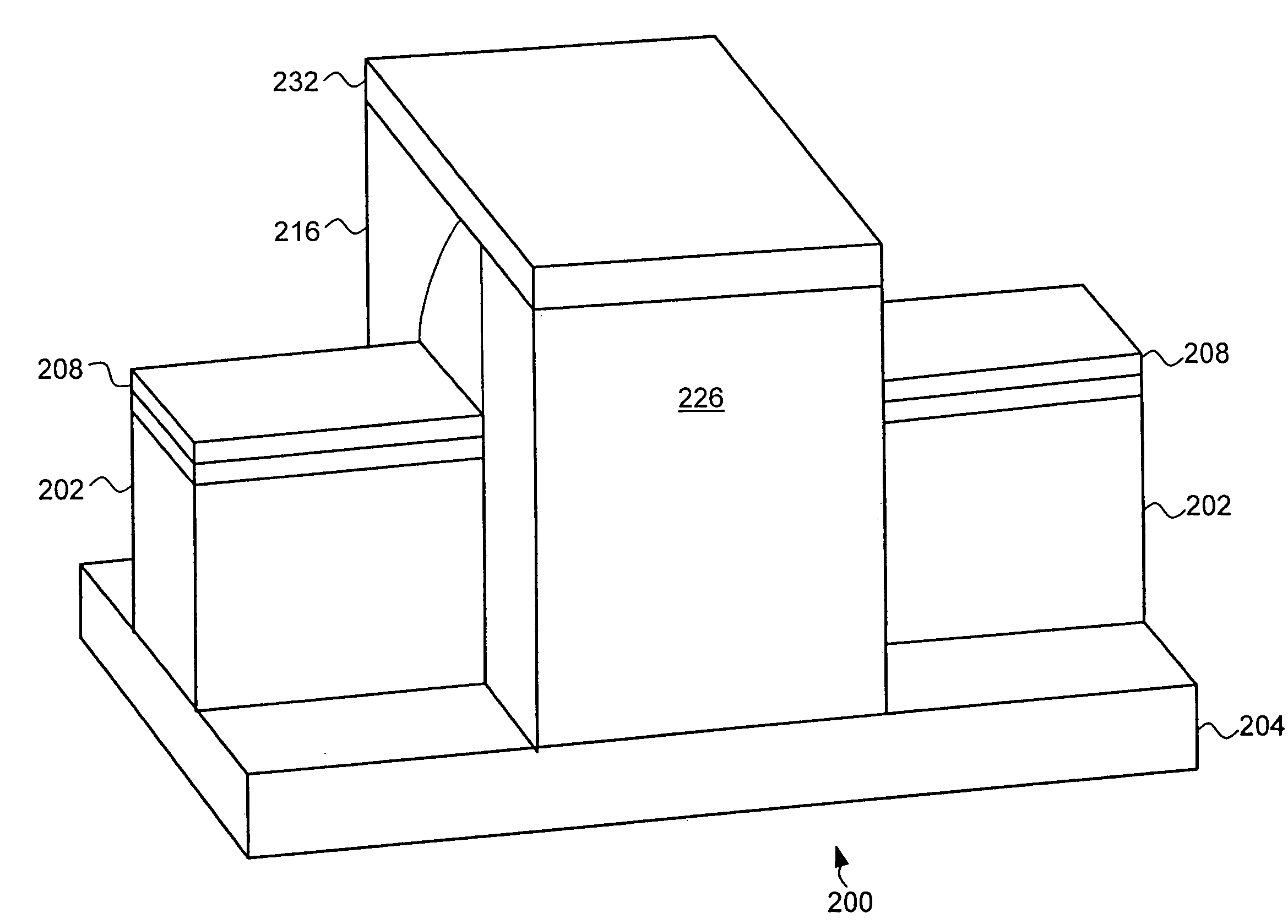
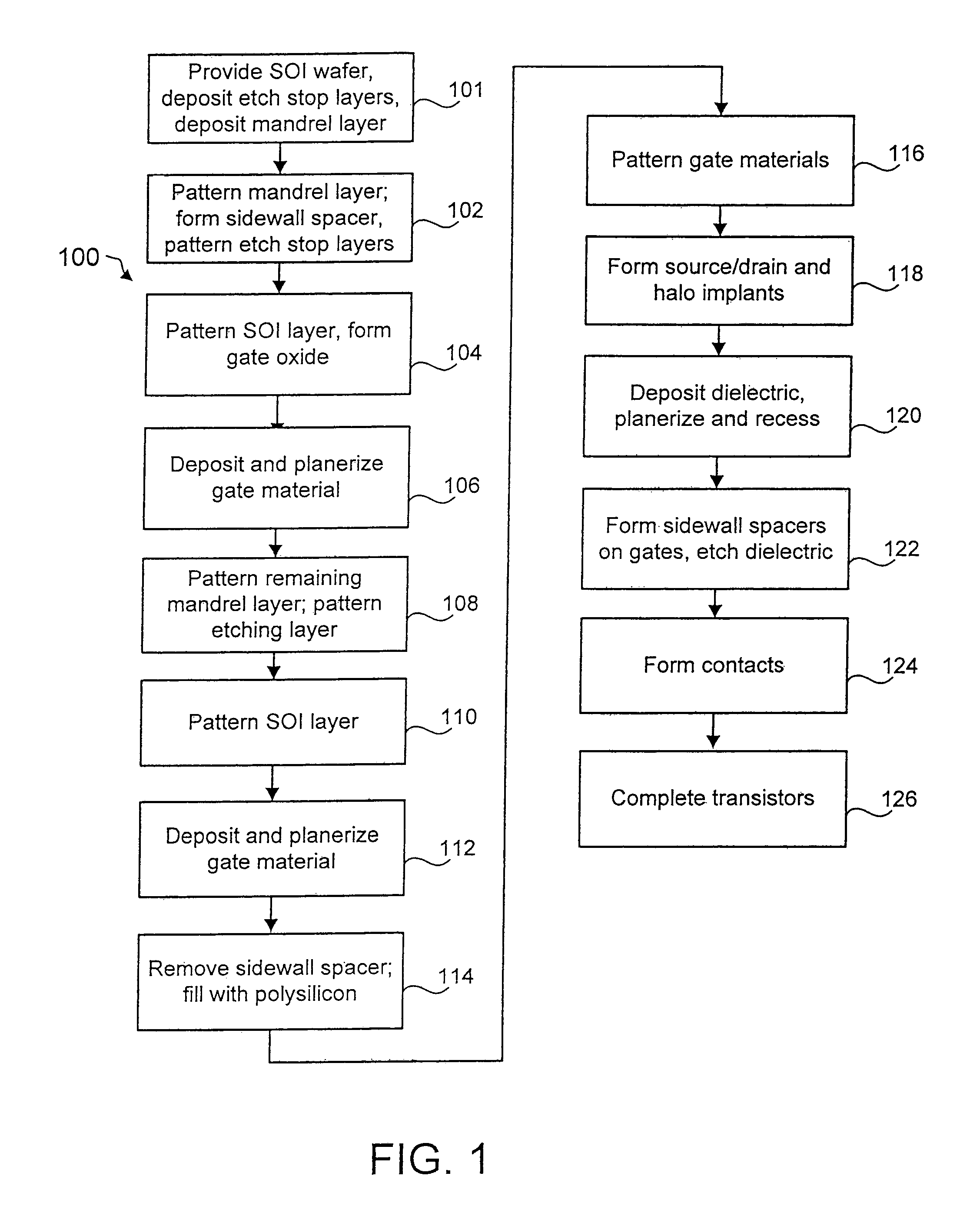
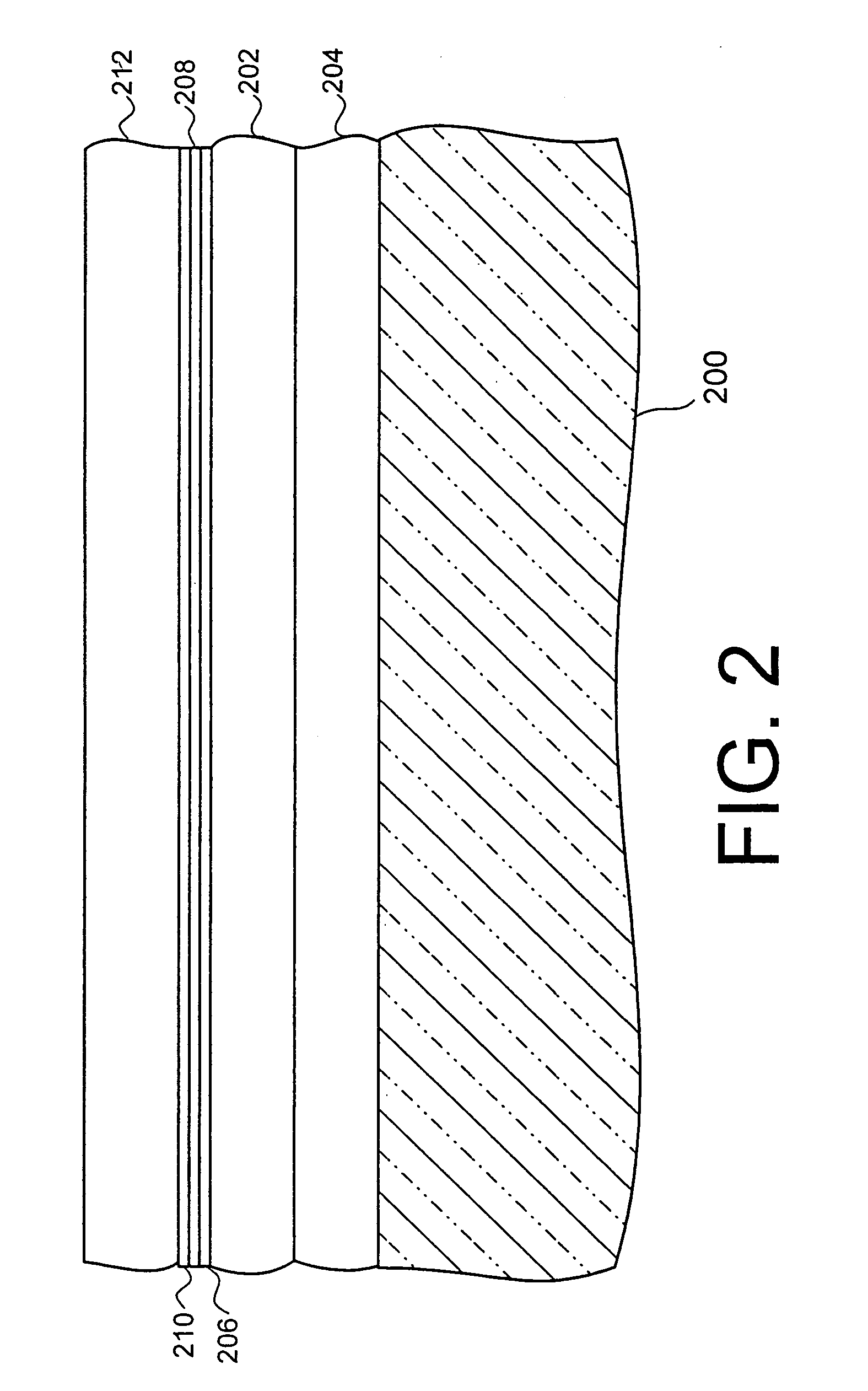
[0020]Accordingly, the present invention provides a double gated transistor and a method for forming the same that results in improved device performance and density. The preferred embodiment of the present invention uses provides a double gated transistor with asymmetric gate doping, where one of the double gates is doped degenerately n-type and the other degenerately p-type. By doping one of the gates n-type, and the other p-type, the threshold voltage of the resulting device is improved. In particular, by asymmetrically doping the two gates, the resulting transistor can, with adequate doping of the body, have a threshold voltage in a range that enables low-voltage CMOS operation. For example, a transistor can be created that has a threshold voltage between 0V and 0.5V for nFETs and between 0 and −0.5V for pFETs.

[0021]The preferred embodiment of the present invention is implemented using a fin type double gated structure. In a fin type structure, the double gates are formed on eac...


PUM


Abstract

Accordingly, the present invention provides a double gated transistor and a method for forming the same that results in improved device performance and density. The preferred embodiment of the present invention uses provides a double gated transistor with asymmetric gate doping, where one of the double gates is doped degenerately n-type and the other degenerately p-type. By doping on of the gates n-type, and the other p-type, the threshold voltage of the resulting device is improved. In particular, by asymmetrically doping the two gates, the resulting transistor can, with adequate doping of the body, have a threshold voltage in a range that enables low-voltage CMOS operation. For example, a transistor can be created that has a threshold voltage between 0V and 0.5V for nFETs and between 0 and −0.5V for pFETs.

Description

[0001]This application is a divisional of Ser. No. 09 / 886,823; filed on Jun. 21, 2001 now U.S. Pat. No. 6,960,806.BACKGROUND OF THE INVENTION[0002]1. Technical Field[0003]The present invention relates generally to the field of semiconductor manufacturing and, more specifically, to a method for forming double gated field effect transistors.[0004]2. Background Art[0005]The need to remain cost and performance competitive in the production of semiconductor devices has caused continually increasing device density in integrated circuits. To facilitate the increase in device density, new technologies are constantly needed to allow the feature size of these semiconductor devices to be reduced.[0006]The push for ever increasing device densities is particularly strong in CMOS technologies, such as the in the design and fabrication of field effect transistors (FETs). FETs are used in almost all types of integrated circuit design (i.e., microprocessors, memory, etc.) Unfortunately, increased de...

Claims


Application Information

Patent Timeline
Patent Type & Authority Patents(United States)
IPC IPC(8): H01L21/84H01L21/336H01L21/8238H01L27/092H01L29/49H01L29/78H01L29/786
CPCH01L21/823842H01L27/092H01L29/785H01L29/66795H01L29/4908H01L21/8238
Inventor BRYANT, ANDRESIEONG, MEIKEIMULLER, K. PAULNOWAK, EDWARD J.FRIED, DAVID M.RANKIN, JED
Owner GLOBALFOUNDRIES INC
Why Eureka
Try Eureka