Dual-port memory array using shared write drivers and read sense amplifiers

a write driver and memory array technology, applied in the direction of information storage, static storage, digital storage, etc., can solve the problems of area or cost sensitive overhead, and achieve the effect of reducing layout area overhead, saving layout area, and reducing the number of write drivers

Inactive Publication Date: 2007-10-30
ALTERA CORP
View PDF34 Cites 10 Cited by
  • Summary
  • Abstract
  • Description
  • Claims
  • Application Information

AI Technical Summary

Benefits of technology

[0014]The present invention provides dual port memory blocks that have a reduced layout area overhead. The write drivers and sense amplifiers are shared between the dual ports to reduce the number of write drivers and sense amplifiers to save layout area.

Problems solved by technology

The overhead becomes more significant for a chip that is area or cost sensitive.

Method used


Image

  • Dual-port memory array using shared write drivers and read sense amplifiers
  • Dual-port memory array using shared write drivers and read sense amplifiers
  • Dual-port memory array using shared write drivers and read sense amplifiers

Examples


Embodiment Construction

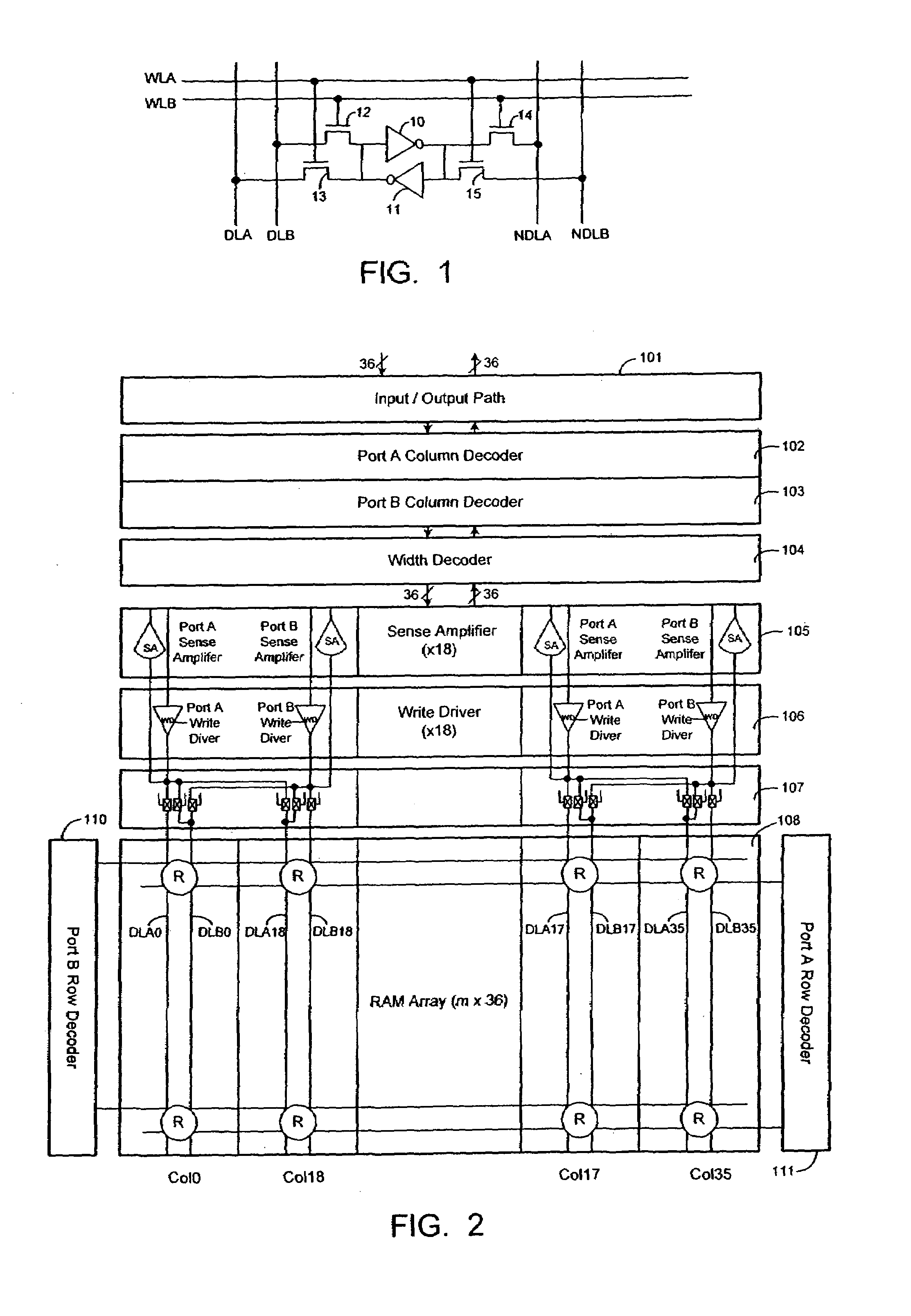
[0025]FIG. 1 illustrates an example of a typical static random access memory (SRAM) cell. The SRAM cell includes cross coupled inverters 10 and 11 and pass transistors 12-15. Inverters 10 and 11 store a bit of digital data. Pass transistors 12-15 control access to inverters 10-11 from word lines for ports A and B (WLA and WLB) and from the differential bitlines for ports A and B (DLA, DLB, NDLA and NDLB).

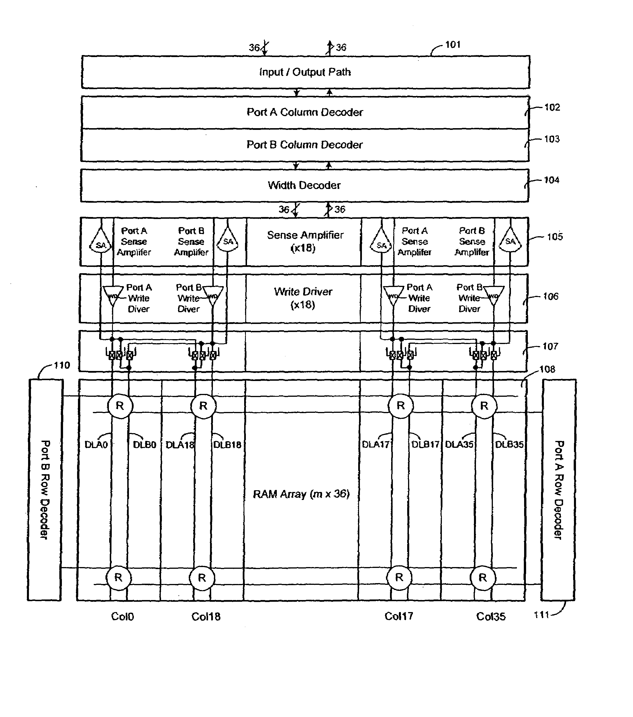
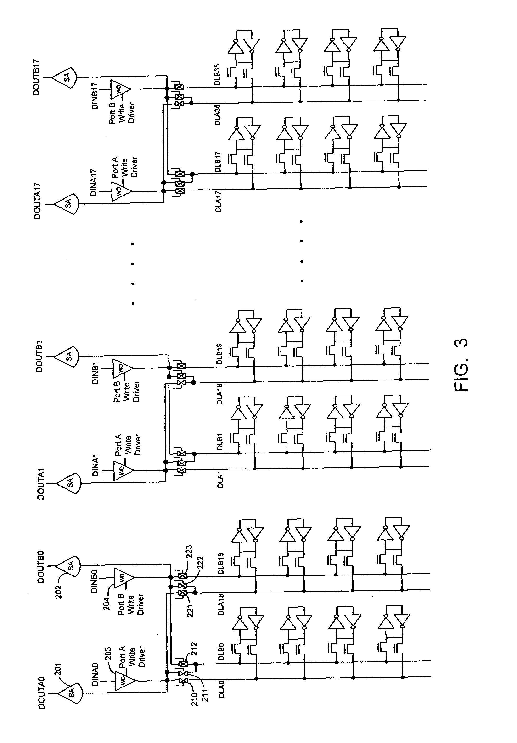
[0026]FIG. 2 illustrates a dual port memory block according to a first embodiment of the present invention. The dual port memory block includes an input / output data path 101 that receives input and output data. The example shown in FIG. 2 includes 36 data input lines and 36 data output lines. The dual port memory block also includes a column decoder 102 for port A, a column decoder 103 for port B, a width decoder 104, a block 105 of sense amplifiers, a block 106 of write drivers, multiplexers 107, an array 108 of memory cells, a row decoder 110 for port B, and a row decoder 111 for ...


PUM


Abstract

Dual port memory blocks that have a reduced layout area are provided. The write drivers and sense amplifiers are shared between the dual ports to reduce the number of write drivers and sense amplifiers to save layout area. The write drivers for the two ports are used to write into all of the first port's bitlines. The sense amplifiers for the two ports are used to read from all of the second port's bitlines. A memory block can to support true dual port (TDP) and simple dual port (SDP) operation using substantially less write drivers and sense amplifiers.

Description

CROSS-REFERENCES TO RELATED APPLICATIONS[0001]This application is a divisional application of U.S. patent application Ser. No. 10 / 928,589 filed Aug. 26, 2004, entitled “DUAL PORT MEMORY ARRAY USING SHARED WRITE DRIVERS AND READ SENSE AMPLIFIERS,” now U.S. Pat. No. 7,110,309 the entire disclosure of which is incorporated by reference for all purposes.BACKGROUND OF THE INVENTION[0002]This invention relates to dual port memory circuits, and more particularly, to dual port memory circuits that have shared write drivers and sense amplifiers.[0003]A configurable memory block in field programmable gate array (FPGA) is usually built to support various read and write operation modes, such as true dual port (TDP), simple dual port (SDP), and single port (SP) modes. The operation mode is configured depending on the user application. A TDP memory supports two write operations, one read and one write operation, or two read operations at one time.[0004]A typical dual port memory has two independe...

Claims


Application Information

Patent Timeline
Patent Type & Authority Patents(United States)
IPC IPC(8): G11C7/10
CPCG11C7/1051G11C7/1069G11C7/1096G11C7/1078G11C7/1075G11C8/16
Inventor YU, HAIMINGKOAY, WEI YEE
Owner ALTERA CORP
Why Eureka
Try Eureka