Light-emitting apparatus with improved bank structure

a technology of light-emitting apparatus and bank structure, which is applied in the direction of discharge tube/lamp details, discharge tube luminescnet screens, electric discharge lamps, etc. it can solve the problems of easy damage to the electrode, easy adhesion of dust on the charged surface, and easy generation of electrostatic discharge, so as to prevent electrostatic discharge damage

Inactive Publication Date: 2007-11-06
SEMICON ENERGY LAB CO LTD
View PDF68 Cites 62 Cited by
  • Summary
  • Abstract
  • Description
  • Claims
  • Application Information

AI Technical Summary

Benefits of technology

[0017]Although the first bank and the second bank may be formed of same materials, it is preferable to use different materials for the first bank and the second bank. In case that an organic compound layer is formed by vapor deposition, it is preferable that the thickness of the first bank be formed to be not more than 1 μm (more preferably, from 0.5 to 1 μm) to prevent the wrap-around of the vapor deposition, since an evaporation mask and the first bank are in contact with each other. Since it is difficult to form a thin film using an organic material, it is preferable to use an inorganic material. In case that a bank is formed of photosensitive resin by exposure, an upper portion is formed to have a curved surface, and a bottom has a width (width of a side of the bank) of 5 μm, or greater than that, which is spread than the upper portion. Consequently, the bank has not less than 10 μm in the width in total, and an aperture ratio is reduced accordingly. According to the present invention, a narrow width bank can be formed, for example, a first bank of 1 μm in width and a second bank of 1 μm in width can be formed to be a 3 μm in width of the banks in total. The width of the second bank may be 0.1 μm, or larger than that, and it is preferable to be larger than the height of the first bank. The width of the second bank may be enough to be about 3 μm to keep sufficient coverage. The reliability of a light-emitting device as a whole is improved by keeping coverage of an organic compound layer and a film formed thereon. The radius of curvature of the upper portion of the second bank may be from 0.5 μm to 2 μm.
[0037]An electrostatic discharge damage can be prevented by forming an antistatic layer that covers an insulating film serving as a second bank. As the antistatic layer, a conductive coated film, for example, a surface-active agent coated film may be utilized. Also, deposited film formed of a material having composition that inorganic salt such as lithium chloride or magnesium chloride is dispersed into film formation material such as synthetic resin or silicate, or deposited film formed of a material having composition that ion-conducting materials such as polymer electrolyte containing a carboxylic acid group or a sulfonic acid group are dispersed into film formation material such as synthetic resin or silicate, or conductive polymer may be utilized as the antistatic layer. After the transportation of the substrate, the antistatic layer is removed, and anisotropic etching is carried out on the insulating film, and then, an organic compound layer is formed.

Problems solved by technology

In case of separating equipment, a problem will arise that substrates should be transported between the installation sites, and there is a risk of electrostatic discharge damage and adhesion of dust on a substrate during transportation of the substrates.
Due to this, there is a threat of adhesion of dust on the charged-surface or generating electrostatic discharge if the substrate, the organic insulating film, and the inorganic insulating film come into contact with another object.
Since an organic compound layer serving as a light-emitting layer has a thin film thickness, poor coverage easily occurs due to large irregularities of the surface, that is, large difference in level is produced.

Method used


Image

  • Light-emitting apparatus with improved bank structure
  • Light-emitting apparatus with improved bank structure
  • Light-emitting apparatus with improved bank structure

Examples


embodiment mode 1

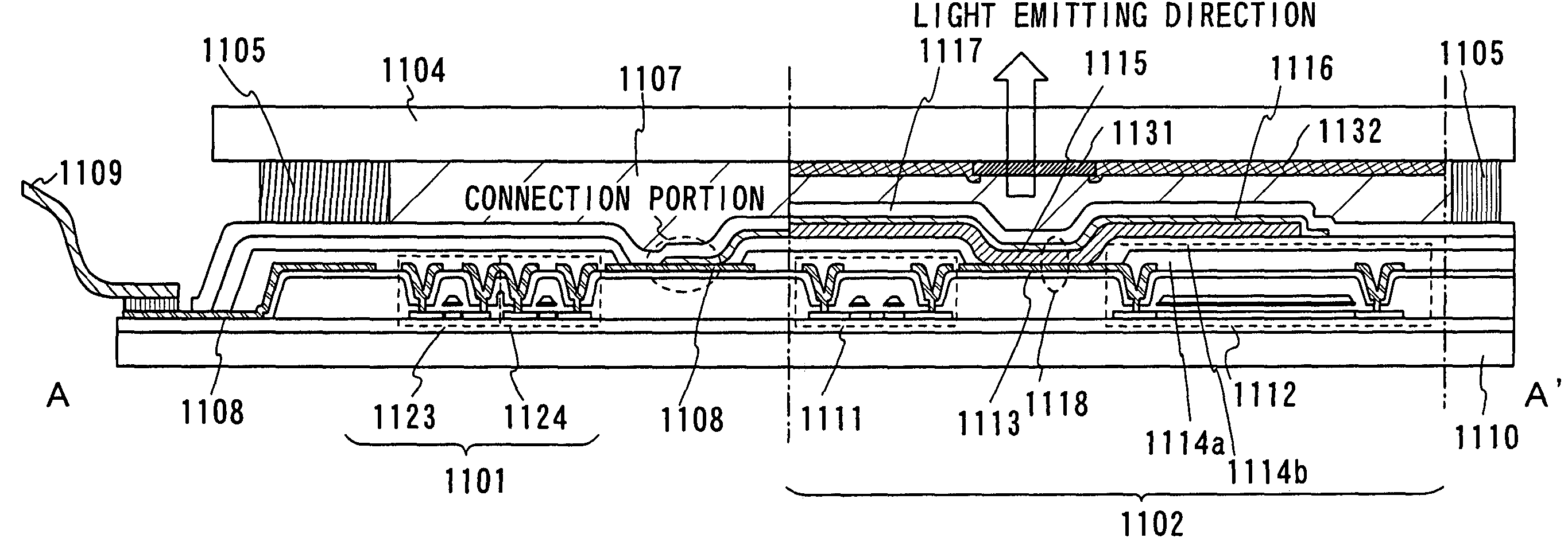
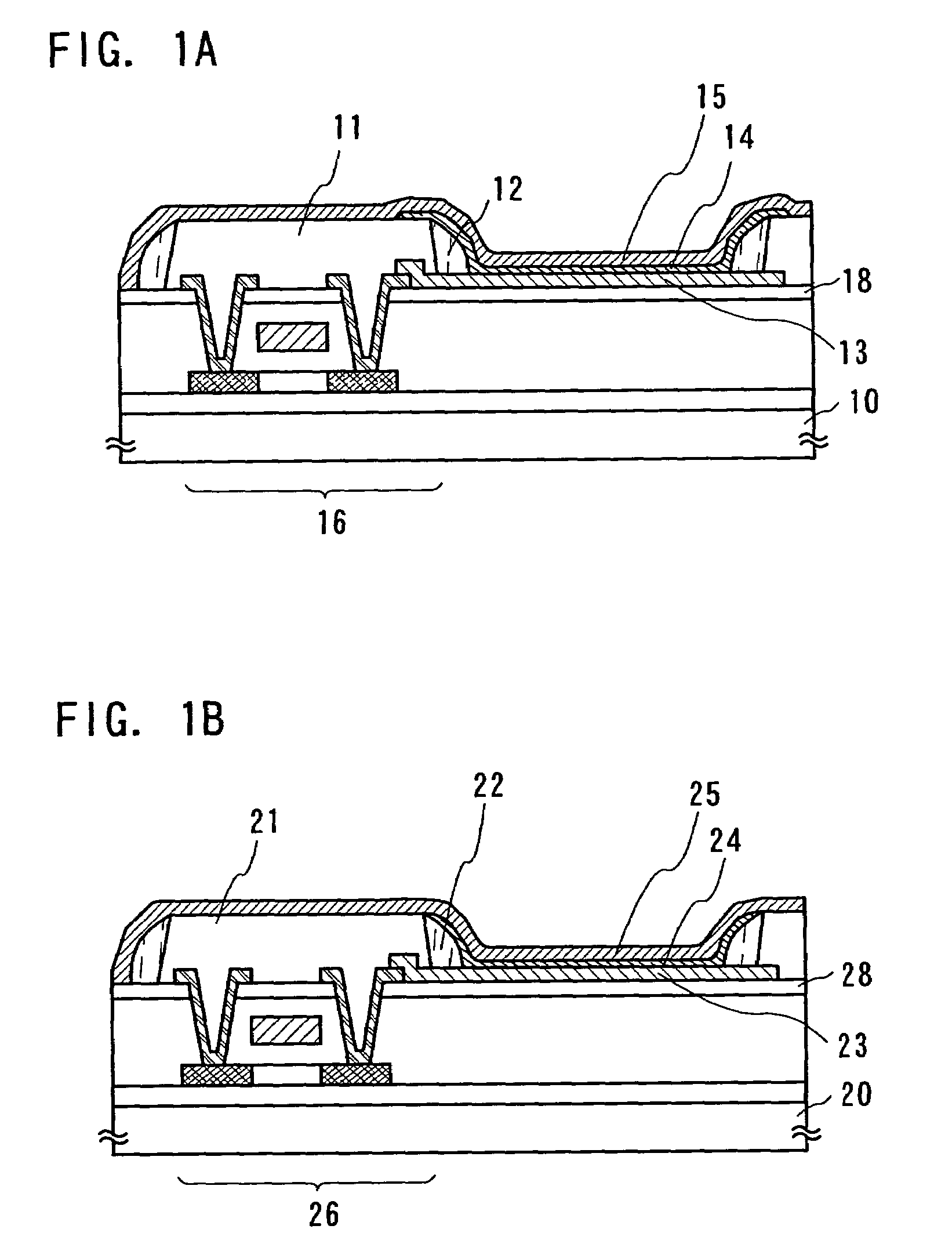
[0065]The present invention is described by using an example of an active matrix light-emitting device in this embodiment mode.

[0066]In FIG. 1A, reference numeral 10 is a substrate, 11 is a first bank, 12 is a second bank, 13 is a first electrode, 14 is an organic compound layer, 15 is a second electrode, 16 is a TFT, and 18 is an insulating film. In FIG. 1A, the electrode 13 serves as an anode of a light-emitting device and the second electrode serves as a cathode of the light-emitting device, but not exclusively, the first electrode can serve as a cathode and the second electrode can serve as an anode if materials are selected appropriately.

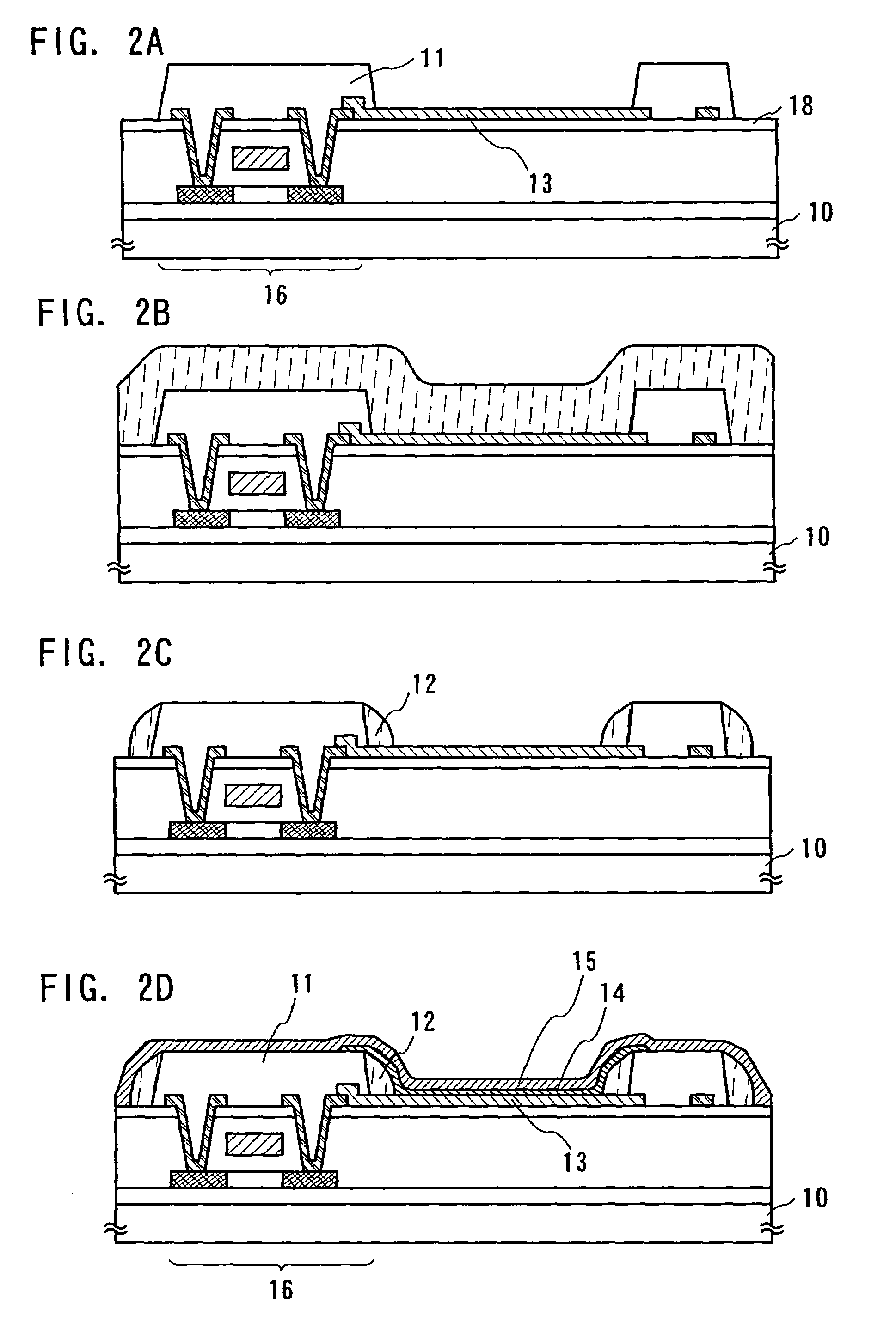
[0067]An example of a fabrication process for forming a structure illustrated in FIG. 1A is shown in FIGS. 2A, 2B, 2C and 2D.

[0068]The TFT 16 is fabricated over the substrate 10 having an insulating surface. As materials for an interlayer insulating film of the TFT, for example, inorganic materials formed by sputtering, PCVD, or coating (silico...

embodiment mode 2

[0086]An example of preventing electrostatic discharge damage of a TFT by forming an antistatic layer during a fabrication process of an active matrix display device will be described with reference to FIGS. 3A, 3B and 3C. In FIGS. 3A, 3B and 3C, like components are denoted by like numerals as of FIG. 1A.

[0087]The TFT 16 and the first electrode 13 are formed over the substrate 10. Then, the first bank 11 to cover the edge portion of the first electrode is formed. (FIG. 3A)

[0088]An insulating film is formed over the whole surface of the substrate, and an antistatic layer 30 is formed thereon. (FIG. 3B) The electrostatic discharge damage can be prevented by forming the antistatic layer 30. Static electricity is easily charged an insulating surface. Due to this, there is a threat of adhesion of dust over the charged-surface or generating electrostatic discharge when touching another objects.

[0089]For forming the antistatic layer 30, poly(ethylenedioxythiophene) / polystyrenesulphonic aci...

embodiment mode 3

[0094]In Embodiment Mode 1, an example of forming the second bank that covers the side face of the first bank was described. In this embodiment mode, an example of forming a second bank that covers all over a first bank will be described with reference to FIG. 4A.

[0095]In FIG. 4A, reference numeral 40 is a substrate, 41 is a first bank, 42 is a second bank, 43 is a first electrode, 44 is an organic compound layer, 45 is a second electrode, 46 is a TFT, and 48a to 48c are insulating films.

[0096]An example of a fabrication process for forming the structure shown in FIG. 4A is illustrated in FIGS. 5A to 5D.

[0097]The TFT 46 is formed over the substrate 40 having an insulating surface. The TFT 46 may be formed to be an n-channel type TFT or a p-channel type TFT by a known method. Reference numeral 46a is a channel formation region, 46b, 46c are a source region or a drain region, 46d is a gate electrode, 46e, 46f are a source electrode or a drain electrode, 46g is a gate insulating film a...


PUM


Abstract

Conventionally, there are problems that high resolution is difficult to be achieved since an extreme narrow width bank can not be formed and an aperture ratio as a light-emitting device is low. In addition, there is a threat of electrostatic discharge damage or adhesion of dust during the transportation of a substrate provided with an anode into the equipment for depositing EL material. In view of the foregoing, a first bank formed of an inorganic insulating film is formed, and an insulating film is formed thereon, then, a second bank in contact with a side face of the first bank by carrying out etch back, and then, a side wall bank is formed. For preventing electrostatic discharge damage, an antistatic layer is formed, and the substrate is transported, then, the antistatic layer is removed to form the second bank.

Description

BACKGROUND OF THE INVENTION[0001]1. Field of the Invention[0002]The present invention relates to a light-emitting apparatus comprising a light-emitting device that emits fluorescence or phosphoresce upon application of an electric field thereto and includes a pair of electrodes and a film containing an organic compound (hereinafter, an organic compound layer) that is sandwiched between the pair of electrodes, and to a method of fabricating the light-emitting apparatus. In this specification, the term “light-emitting apparatus” includes an image display apparatus, a light-emitting device, or a light source (including a lighting system). Also, the following modules are included in the light-emitting apparatus: a module obtained by attaching a connector such as an FPC (flexible printed circuit), a TAB (tape automated bonding) tape, or a TCP (tape carrier package) to a light-emitting device; a module obtained by providing a PWB (printed wiring board) with a tip of a TAB tape or a TCP; a...

Claims


Application Information

Patent Timeline
Patent Type & Authority Patents(United States)
IPC IPC(8): H01J1/62H01L27/32H05B33/22
CPCH05B33/22H01L27/3246H10K59/122H05B33/10
Inventor KUWABARA, HIDEAKI
Owner SEMICON ENERGY LAB CO LTD
Why Eureka
Try Eureka