Circuit substrate

a technology of circuit substrate and substrate layer, which is applied in the direction of film/foil adhesive, conductive pattern formation, non-printed circuit electrical components association, etc., can solve the problems of complex manufacturing process and circuit substrate becoming expensive unavoidably, and achieves simple arrangement, easy and fast inspection of bonded states, and high reliability in the connected state

Inactive Publication Date: 2007-11-06
SONY CORP
View PDF17 Cites 18 Cited by
  • Summary
  • Abstract
  • Description
  • Claims
  • Application Information

AI Technical Summary

Benefits of technology

[0009]The problems that the present invention intends to solve are that the related-art printed circuit wiring board needs a large number of manufacturing processes, the manufacturing process is complex and that a circuit substrate becomes expensive unavoidably. However, according to the present invention, it is possible to easily manufacture a circuit substrate by a simple manufacturing process in which a flexible substrate is sandwiched by two rigid substrates. Therefore, according to the present invention, it becomes possible to manufacture a circuit substrate with a simple arrangement and which is highly reliable in practical use.
[0011]According to the circuit substrate of the present invention, it becomes possible to easily and quickly inspect the bonded states of a plurality of land portions by which the rigid substrates and the flexible wiring board are electrically connected to each other by X-ray photographs obtained from taking an X-ray of the bonded states and it is possible to provide a circuit substrate having a simple arrangement which is highly reliable in the connected state of the connected portion.
[0012]The bonded states of a plurality of land portions can be easily and quickly inspected by taking an X-ray of the bonded states and a circuit substrate which is highly reliable in the connected state of the connected portion can be realized by a simple arrangement.

Problems solved by technology

The problems that the present invention intends to solve are that the related-art printed circuit wiring board needs a large number of manufacturing processes, the manufacturing process is complex and that a circuit substrate becomes expensive unavoidably.

Method used


Image

  • Circuit substrate
  • Circuit substrate
  • Circuit substrate

Examples


Embodiment Construction

[0029]Before describing the preferred embodiments of the present invention, the present invention may be summarized such that a circuit substrate in which bonded states of a plurality of land portions can be checked easily and quickly by a suitable method such as X-ray photographs and which is highly reliable in the connected states of the connection portions could be realized by a simple arrangement.

[0030]The embodiments of the present invention will be described below with reference to the accompanying drawings.

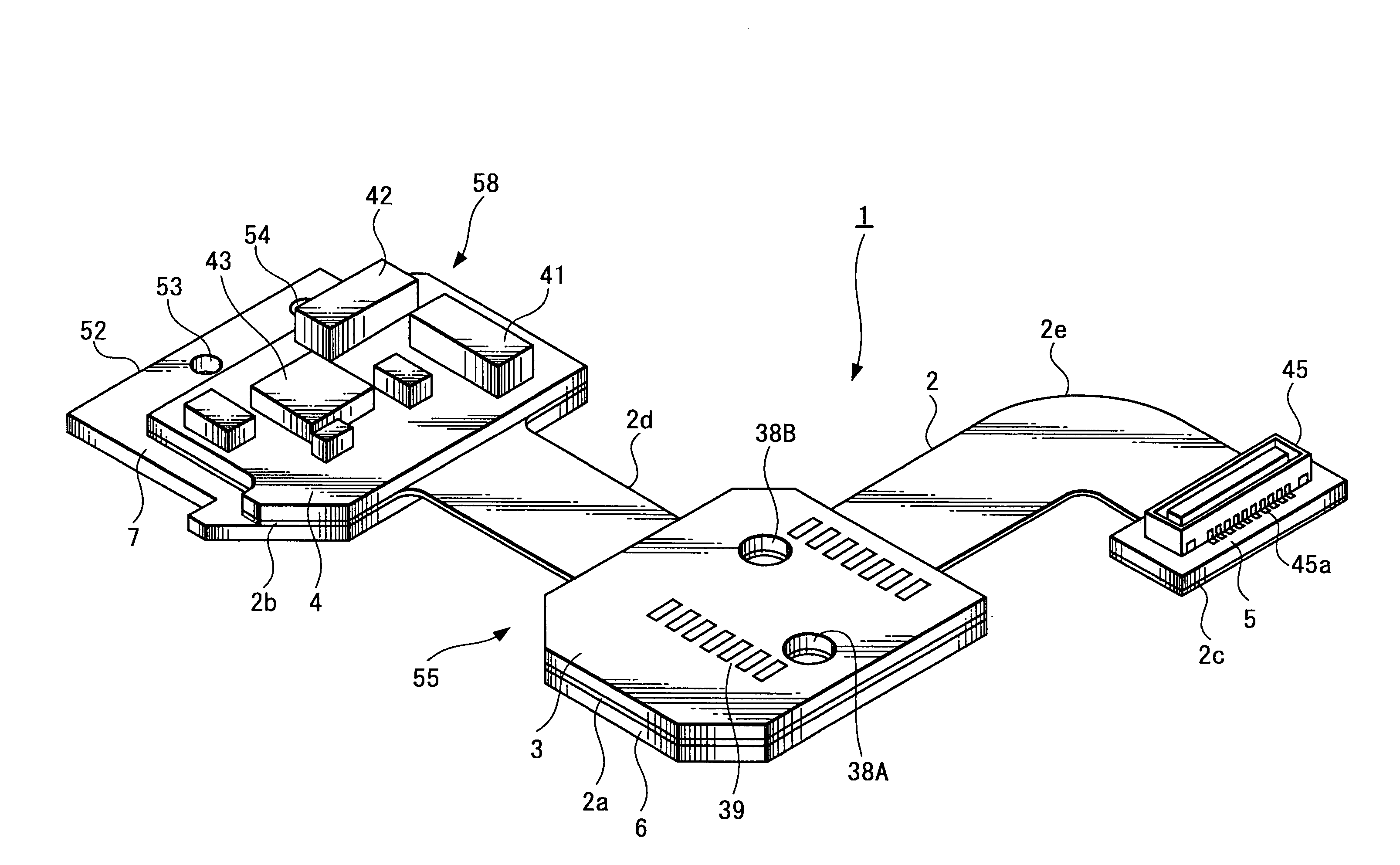
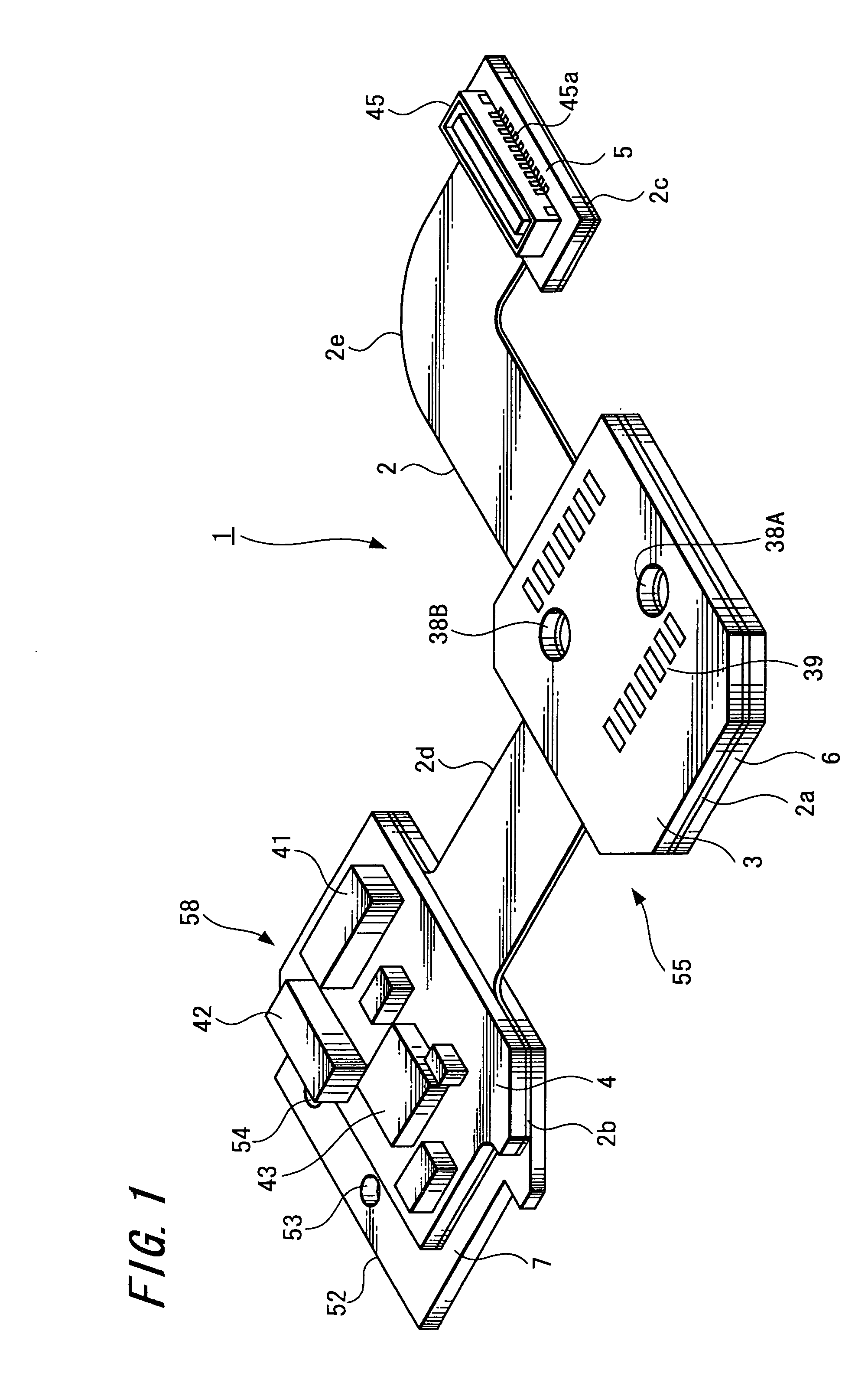
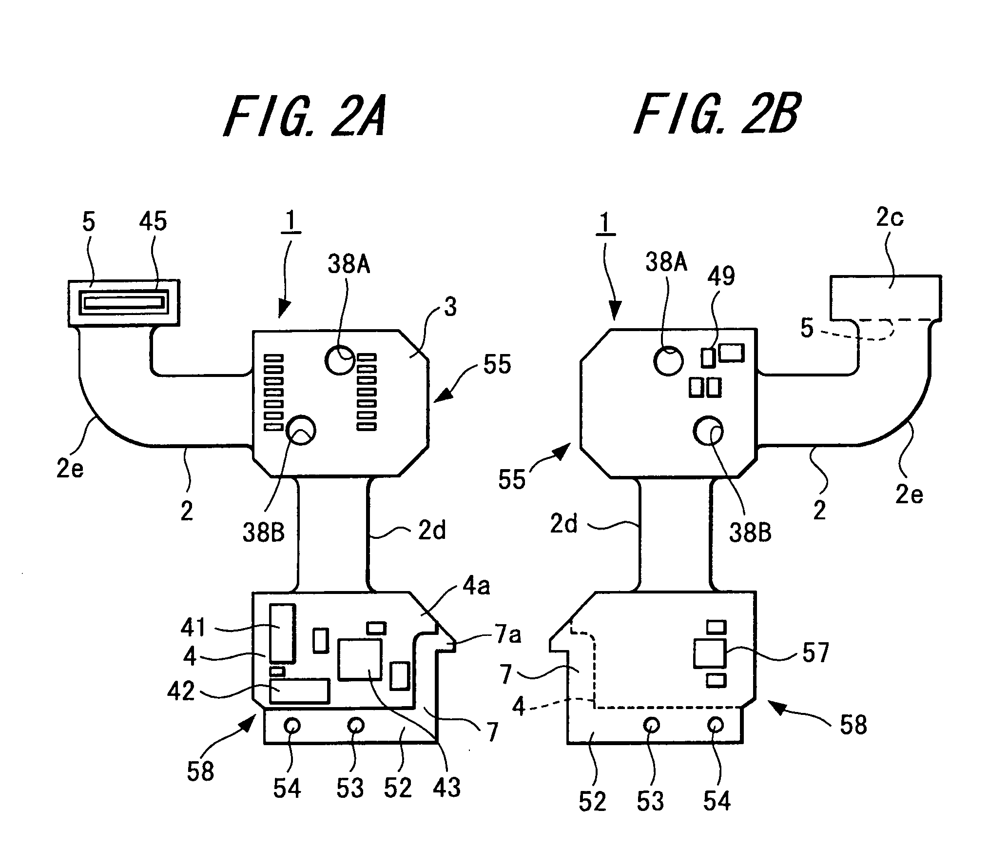
[0031]FIGS. 1 to 16 are diagrams used to explain the embodiments of the present invention. More specifically, FIG. 1 is a perspective view of an external appearance of a circuit substrate according to a first embodiment of the present invention. FIGS. 2A and 2B are a front view and a back view of the same circuit substrate, respectively. FIGS. 3A and 3B are a front view and a back view of a flexible wiring board, respectively. FIG. 4 is a front view of a first printed wirin...


PUM

PropertyMeasurementUnit
lengthaaaaaaaaaa
lengthaaaaaaaaaa
distanceaaaaaaaaaa

Abstract

A circuit substrate includes a first rigid substrate having a plurality of land portions located at a predetermined interval on one surface, a second rigid substrate having a plurality of second land portions located at a predetermined interval on one surface and a flexible wiring board sandwiched by the first and second rigid substrates and which has a plurality of third land portions corresponding to the first land portions on one surface and a plurality of fourth land portions corresponding to the second land portions on the other surface. In this circuit substrate, the second and fourth land portions are displaced from each other relative to the first and third land portions and at least part of the first and third land portions and at least part of the second and fourth land portions are electrically connected to each other, respectively.

Description

CROSS REFERENCES TO RELATED APPLICATIONS[0001]The present invention contains subject matter related to Japanese Patent Application JP 2005-252888 filed in the Japanese Patent Office on Aug. 31, 2005, the entire contents of which being incorporated herein by reference.BACKGROUND OF THE INVENTION[0002]1. Field of the Invention[0003]The present invention relates to a circuit substrate in which high-density mounting can be realized by integrally sandwiching a flexible wiring board with two rigid substrates.[0004]2. Description of the Related Art[0005]Cited Patent Reference 1, for example, describes an example of this kind of circuit substrate. The Cited Patent Reference 1 describes a method of manufacturing a printed circuit wiring board in which a flexible substrate is sandwiched by rigid substrates. A method of manufacturing a printed circuit wiring board described in the Cited Patent Reference 1 includes a rigid substrate forming process for forming a rigid substrate in which a first...

Claims


Application Information

Patent Timeline
Patent Type & Authority Patents(United States)
IPC IPC(8): H05K7/00
CPCH05K1/189H05K1/147H05K1/141Y10T29/49126H05K3/363H05K3/4691H05K2201/09063H05K2201/2009H05K2203/1572H05K2203/167Y10T29/49155Y10T156/137Y10T156/1075Y10T156/1056Y10T29/49139Y10T29/4913
Inventor URUSHIBARA, TOSHICHIKASHIOZAWA, KOJIOKABE, MASAKAZUHYODO, YUKIKOMASUDA, YUSUKEMIYAMOTO, TADAYUKI
Owner SONY CORP
Why Eureka
Try Eureka