Hot carrier circuit reliability simulation

a hot carrier circuit and reliability simulation technology, applied in the direction of electric/magnetic computing, instruments, analogue processes for specific applications, etc., can solve the problems of pmos transistor b>10/b> deterioration due to device aging, oxide/silicon interface above channel region damage, and the design of such circuits is extremely complicated. , to achieve the effect of reducing the time required

Inactive Publication Date: 2007-11-06
CADENCE DESIGN SYST INC
View PDF21 Cites 31 Cited by
  • Summary
  • Abstract
  • Description
  • Claims
  • Application Information

AI Technical Summary

Benefits of technology

[0017]The present invention is directed to a number of improvements in methods for reliability simulations in aged circuits whose operation has been degraded through hot-carrier or other effects. According to a first aspect, the circuit operation at a plurality of different circuit ages or stress times can be performed within a single simulation, greatly reducing the time required over what would be needed if each circuit stress time were to be simulated separately.
[0022]In a further aspect of the present invention, the device characterization means, the device estimation means, the device degradation quantization means, the circuit netlist generation for aging simulation, and other features can be embedded into the circuit simulator. This will improve simulation efficiency and capability still further.

Problems solved by technology

The design of such circuits is extremely complicated and usually employs simulators, such as SPICE, to predict circuit operation.
With operation over time, the PMOS transistor 10 will suffer degradation due to device aging.
Additionally, the oxide / silicon interface above channel region is damaged by the more energetic holes and electrons.
These effects degrade the transistor's operation in several ways.
The strength of these effects depend differently on bias conditions, but traditionally the change due to lower mobility has been smaller; however, as device sizes have decreased, this interface damage becomes more significant and, depending upon bias conditions, often becomes the larger effect below a quarter micron or so.
These problems are aggravated as device sizes decrease into the submicron region.
These hot electron effects build up over time causing the device to degrade as it ages.
However, the same aged model card can no longer be used for all of the similar devices.
As a real circuit will often contain thousands or even millions of elements, the simulation of the aging of such circuits is a extremely complicated process for which a large number of improvements are desirable.

Method used


Image

  • Hot carrier circuit reliability simulation
  • Hot carrier circuit reliability simulation
  • Hot carrier circuit reliability simulation

Examples


Embodiment Construction

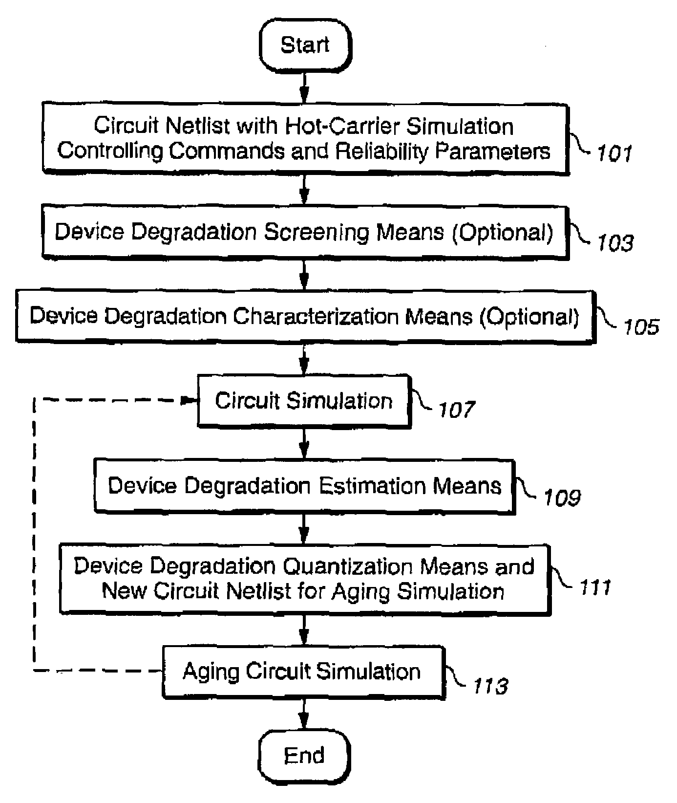
[0033]The various aspects of the present invention will be described with respect to the flow chart of FIG. 5. As described in the following, this flow differs from the prior art methods in some of the steps included as well as in the details of some of the steps that are found in the prior art. Although the discussion is mainly in terms of aging due to hot carriers, the techniques generally apply to circuit degradation due to the degradation of its constituent devices from other mechanisms.

[0034]Step 101 provides the netlist describing the circuit that will have the simulation controlling commands and reliability parameters of the present invention. This will include the various connections of the circuit elements and model cards for these elements as well as the age models. The age models may be those that are described in provisional U.S. patent application Ser. No. 60 / 236,587, entitled “Hot-Carrier Device Degradation Modeling and Extraction Methodologies”, filed 29 Sep. 2000, wh...


PUM


Abstract

The present invention is directed to a number of improvements in methods for reliability simulations in aged circuits whose operation has been degraded through hot-carrier or other effects. A plurality of different circuit stress times can be simulated within a single run. Different aging criteria may be used for different circuit blocks, circuit block types, devices, device models and device types. The user may specify the degradation of selected circuit blocks, circuit block types, devices, device models and device types independently of the simulation. Device degradation can be characterized in tables. Continuous degradation levels can be quantized. Techniques are also described for representing the aged device in the netlist as the fresh device augmented with a plurality of independent current sources connected between its terminals to mimic the effects of aging in the device. The use of device model cards with age parameters is also described. To further improve the circuit reliability simulation, a gradual or multi-step aging is used instead of the standard one step aging process. Many of these features can be embedded within the circuit simulator. A user data interface is also presented to implement these techniques and further allow users to enter their device models not presented in the simulator. For example, a proprietary model of, say, the substrate current in an NMOS could used be with a SPICE simulator employing a different model to simulate the aging of the circuit.

Description

CROSS REFERENCE TO RELATED APPLICATIONS[0001]This application claims priority from provisional U.S. patent applications: Ser. No. 60 / 236,865, entitled “Hot-Carrier Circuit Reliability Simulation”, filed 29 Sep. 2000; 60 / 236,587, entitled “Hot-Carrier Device Degradation Modeling and Extraction Methodologies”, filed 29 Sep. 2000; and 60 / 236,586, entitled “Hot-Carrier Reliability Design Rule Checker”, filed 29 Sep. 2000.[0002]The above referenced applications are incorporated herein by reference for all purposes. The prior applications, in some parts, may indicate earlier efforts at describing the invention or describing specific embodiments and examples. The present invention is, therefore, best understood as described herein.FIELD OF THE INVENTION[0003]This invention relates generally to a design aiding apparatus and methods for the design of integrated circuits, and, more specifically, to methods for simulating the time degradation of a circuit due to the hot carrier effect.Copyrigh...

Claims


Application Information

Patent Timeline
Patent Type & Authority Patents(United States)
IPC IPC(8): G06F17/50G06F9/44
CPCG06F17/5036G06F30/367
Inventor WU, LIFENGLIU, ZHIHONGCHEN, ALVIN I.CHOI, JEONG Y.MCGAUGHY, BRUCE W.
Owner CADENCE DESIGN SYST INC
Why Eureka
Try Eureka