Field emission display having emitter arrangement structure capable of enhancing electron emission characteristics

a carbon nanotube and emission display technology, applied in the field of field emission display, can solve the problems of high technology, complicated production, and high equipment requirements, and achieve the effect of improving the efficiency of the emission display and enhancing the electron emission characteristics

Inactive Publication Date: 2007-11-27
SAMSUNG SDI CO LTD
View PDF14 Cites 8 Cited by
  • Summary
  • Abstract
  • Description
  • Claims
  • Application Information

AI Technical Summary

Benefits of technology

[0011]An aspect of the present invention is to provide a field emission display that enables electrons emitted from emitters to land on intended phosphors without undergoing scattering.
[0012]Another aspect of the present invention is to provide a field emission display that increases electron emission levels.
[0013]Yet another aspect of the present invention is to provide a field emission display that increases the number of unit pixels within a display region.

Problems solved by technology

Not only is production complicated and a high technology is needed, but expensive equipment is also required, thereby increasing overall unit costs.
These factors make the mass production of such FEDs problematic.
However, it is difficult to precisely form the emitters in holes formed in an insulation layer, which is provided under the gate electrodes.
This is a result of the difficulties involved in forming the emitters with a printing process that uses paste.
In particular, it is very difficult to provide the paste in the minute holes for formation of the emitters.
Further, with respect to the FED having the conventional triode structure, when the electrons emitted from the emitters form electron beams and travel in this state toward their intended phosphors, there are instances when an excessive diverging force of the electron beams is given by the gate electrodes when passing a region of the gate electrodes to which a positive voltage is applied.
In such a case, the electron beam emitted from an emitter illuminates a phosphor adjacent to the intended phosphor as a result of the undesirable re-direction of the electron beams.
This reduces color purity and overall picture quality of the FED.

Method used


Image

  • Field emission display having emitter arrangement structure capable of enhancing electron emission characteristics
  • Field emission display having emitter arrangement structure capable of enhancing electron emission characteristics
  • Field emission display having emitter arrangement structure capable of enhancing electron emission characteristics

Examples


Embodiment Construction

[0028]Reference will now be made in detail to the embodiments of the present invention, examples of which are illustrated in the accompanying drawings, wherein like reference numerals refer to like elements throughout. The embodiments are described below to explain the present invention by referring to the figures.

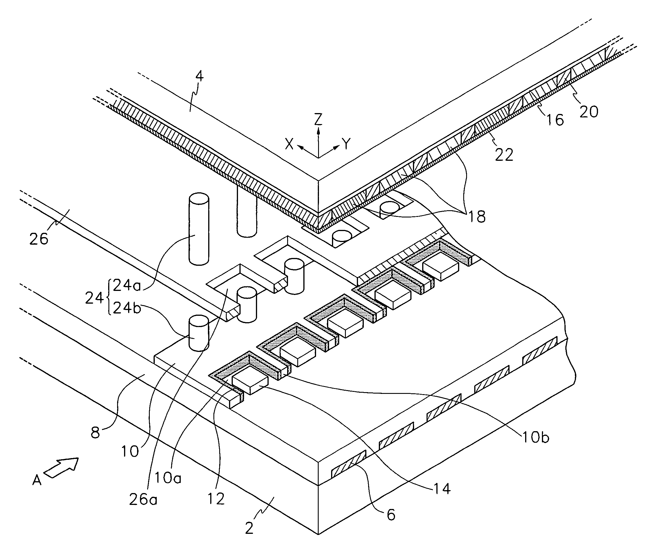
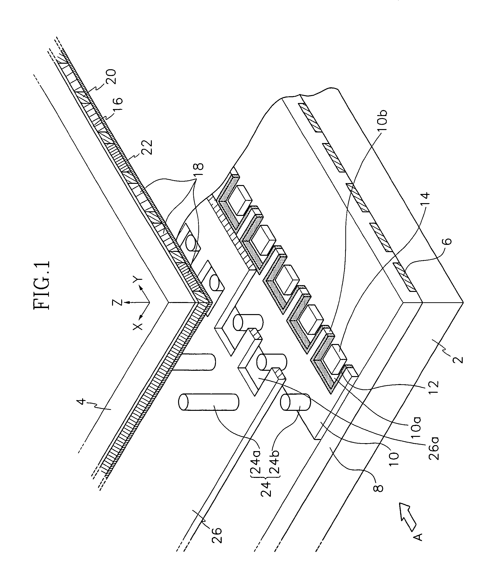
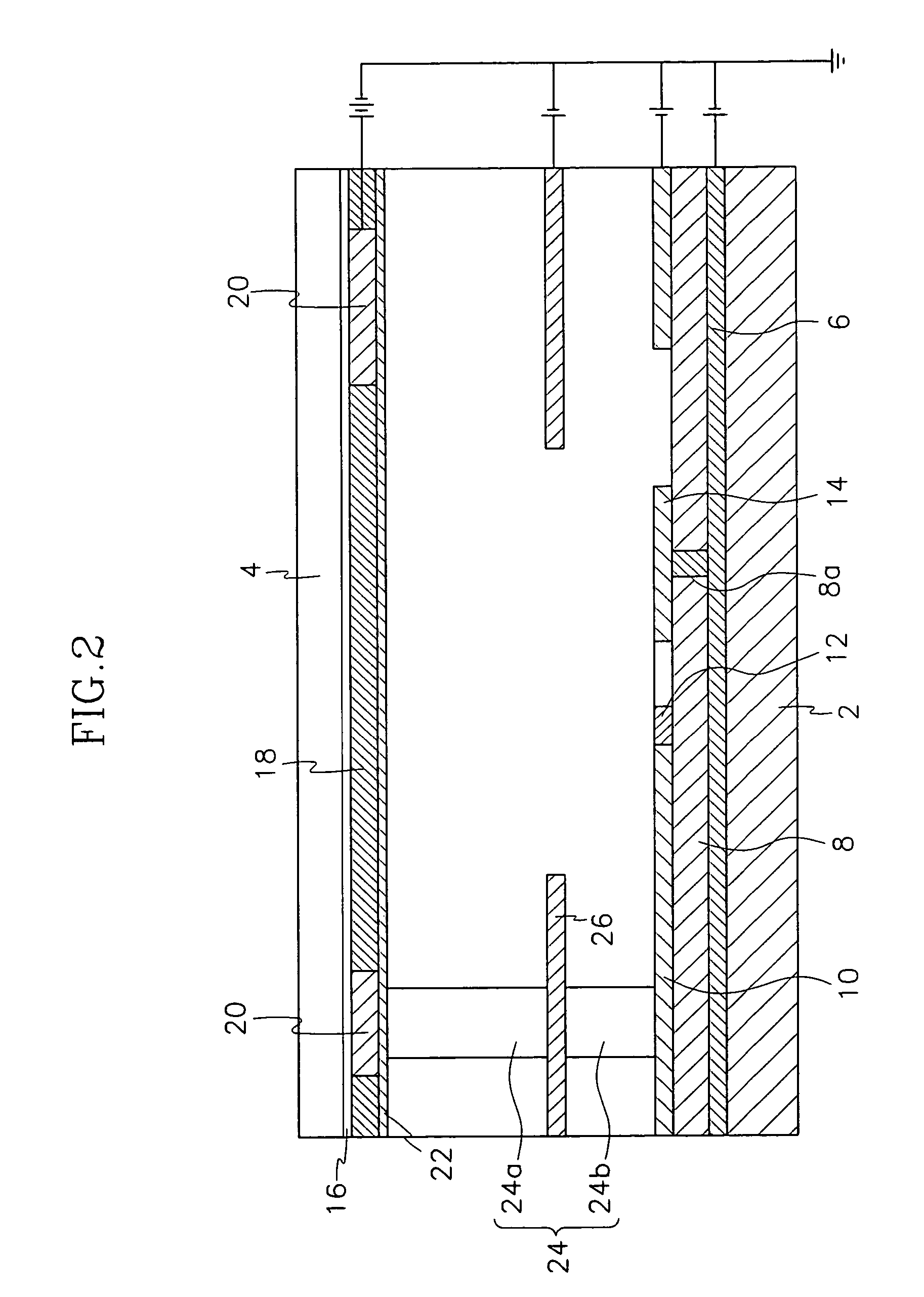
[0029]FIG. 1 is a partial exploded perspective view of a field emission display according to an embodiment of the present invention, and FIG. 2 is a sectional view of the field emission display of FIG. 1 shown in an assembled state. FIG. 2 is shown from direction A of FIG. 1.

[0030]With reference to the drawings, the field emission display (FED) includes a first substrate 2 of predetermined dimensions (hereinafter referred to as a rear substrate) and a second substrate 4 of predetermined dimensions (hereinafter referred to as a front substrate). The front substrate 4 is provided substantially in parallel to the rear substrate 2 with a predetermined gap therebetween. The fro...


PUM


Abstract

A field emission display includes a first substrate, at least one gate electrode formed on the first substrate, cathode electrodes formed on the first substrate, an insulation layer formed between the at least one gate electrode and the cathode electrodes, emitters electrically contacting the cathode electrodes, and formed in pixel regions of the first substrate, counter electrodes electrically connected to the at least one gate electrode and provided such that the counter electrodes and emitters have a first predetermined gap therebetween, a second substrate provided opposing the first substrate with a second predetermined gap therebetween, wherein emitter-receiving sections are provided in the cathode electrodes, dividers are formed between the emitter-receiving sections, the emitters are electrically contacted with an edge of the cathode electrodes corresponding to a shape of the emitter-receiving sections, and at least a part of each of the counter electrodes is provided within the corresponding emitter-receiving sections.

Description

CROSS-REFERENCE TO RELATED APPLICATIONS[0001]This application claims the benefit of Korean Application No. 2003-2412 filed Jan. 14, 2003, in the Korean Intellectual Property Office, the disclosure of which is incorporated herein by reference.BACKGROUND OF THE INVENTION[0002]1. Field of the Invention[0003]The present invention relates to a field emission display, and, more particularly, to a field emission display having carbon nanotube emitters.[0004]2. Description of the Related Art[0005]The field emission display (FED) uses cold cathodes as the source for emitting electrons to realize images. The overall quality of the FED depends on the characteristics of emitters, which form an electron-emitting layer. The first FEDs utilized emitters made mainly of molybdenum (Mo), that is, the emitters were formed of what are referred to as Spindt-type metal tips. As an example of such conventional technology, a display system that has field emission cathodes is disclosed in U.S. Pat. No. 3,78...

Claims


Application Information

Patent Timeline
Patent Type & Authority Patents(United States)
IPC IPC(8): H01J1/30H01J1/304H01J19/02H01J31/12
CPCH01J31/127H01J2329/00H01J2201/304C01B32/05H01J1/30
Inventor KANG, JUNG-HOCHOI, YONG-SOOJIN, SUNG-HWAN
Owner SAMSUNG SDI CO LTD
Why Eureka
Try Eureka