Semiconductor memory device comprising controllable threshould voltage dummy memory cells

a memory cell and semiconductor technology, applied in static storage, digital storage, instruments, etc., can solve the problems of low patterning precision, unstable wlm at both ends of a memory block, and defect detection, so as to reduce the width of a word line, suppress a defect, and improve yield

Inactive Publication Date: 2007-11-27
RENESAS ELECTRONICS CORP
View PDF10 Cites 32 Cited by
  • Summary
  • Abstract
  • Description
  • Claims
  • Application Information

AI Technical Summary

Benefits of technology

[0035]Thus, the present invention can achieve a semiconductor memory device capable of suppressing a defect caused by reduction in width of a word line and falling of a word line which occurs due to disturbance in regularity of intervals of word line patterns near a select transistor in each of memory blocks in a memory cell array having a hierarchical bit line structure, and realizing a chip having improved yield and high reliability.

Problems solved by technology

It causes a problem such that patterning of the word lines of, for example, WL0 or WLm at both ends of a memory block is unstable, that is, patterning precision is lower as compared with that of word lines of, for example, WL1 to WLm-1 in the center of the memory block, in which regularity of the wiring arrangement is maintained.
Further, when a word line having a very small width is formed, there is the possibility that the word line falls and is short-circuited with a neighboring word line or the gate line of a select transistor, and a defect occurs.
Such a problem may similarly occurs in the memories disclosed in JP-A No. 2001-156275 and Y. Sasago et al, “IEEE International Electron Devices Meeting”, 2003, pp.
Further, such a problem may similarly occur not only in an AND cell type EEPROM but also in an NAND cell type EEPROM disclosed by, for example, F. Arai et al, “IEEE International Electron Devices Meeting”, 2000, pp.
It causes a problem such that patterning of the word lines of, for example, WL0 and WLm at both ends of a memory block is unstable, that is, patterning precision is lower as compared with that of word lines of, for example, WL1 to WLm-1 in the center of the memory block, in which regularity of the wiring arrangement is maintained.
Therefore, like the AND cell type EEPROM, the NAND cell type EEPROM has a problem of reduction in the word line width and falling of the word line in an end of each memory block.
In this case, characteristics of writing, erasing, and the like of memory cells are largely different from those of memory cells of other word lines, and an operation error may occur.
When the line width is decreased severely, there is the possibility that a word line falls and is short-circuited with a neighboring word line or a gate signal of a select transistor, thereby causing a defect.

Method used


Image

  • Semiconductor memory device comprising controllable threshould voltage dummy memory cells
  • Semiconductor memory device comprising controllable threshould voltage dummy memory cells
  • Semiconductor memory device comprising controllable threshould voltage dummy memory cells

Examples


first embodiment

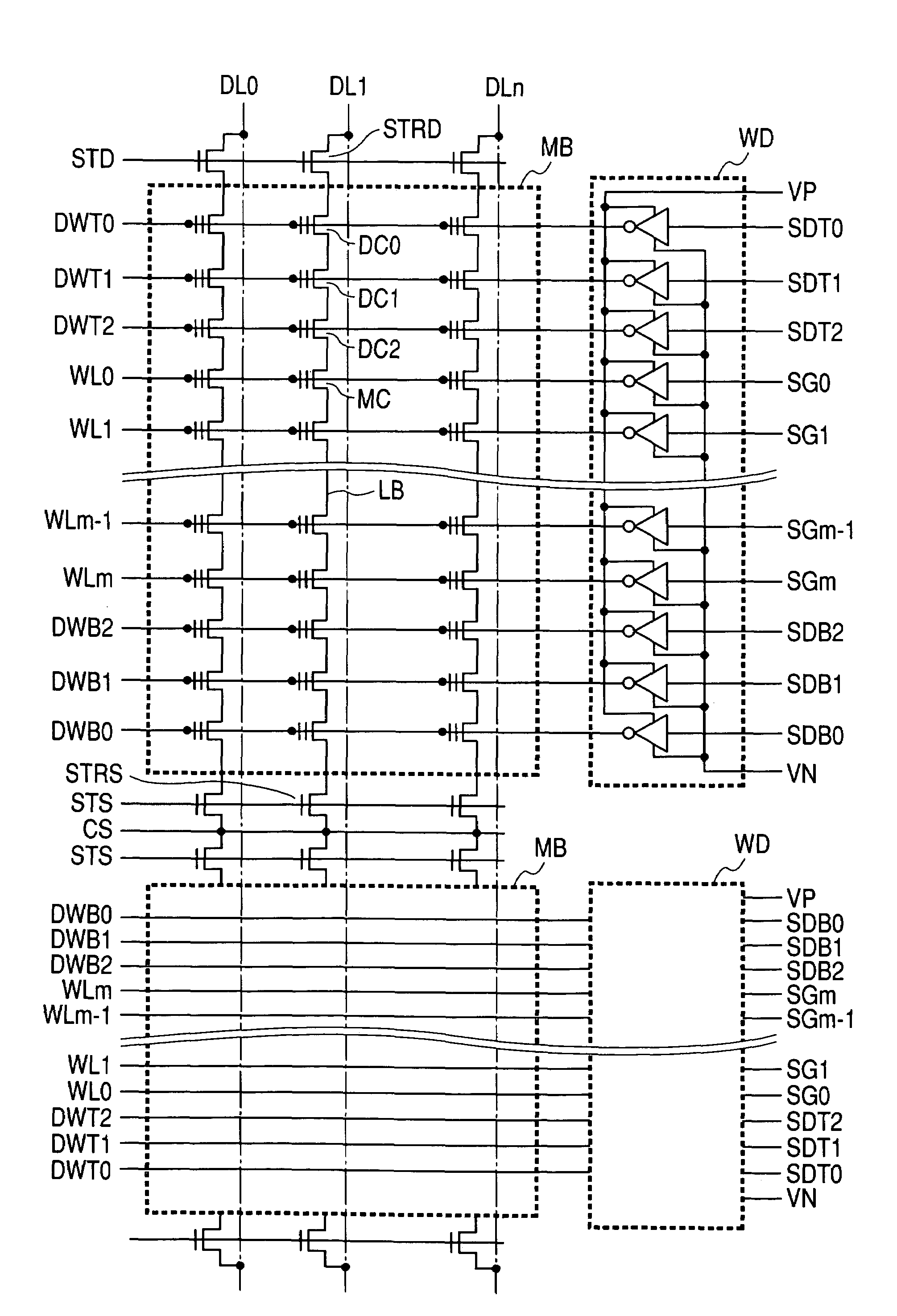
[0068]FIG. 4 illustrates a semiconductor memory device according to a first embodiment of the invention. A memory cell array shown in FIG. 4 has a hierarchical bit line structure. A memory block MB in the diagram may be of the AND cell type or the NAND cell type. The memory block MB is different from a conventional AND type or NAND type memory block is with respect to the point that dummy word lines DWT0 to DWT2 and DWB0 to DWB2 are provided on the outside of word lines WL0 to WLm. There is the possibility that the patterning precision of a word line pattern disposed at an end of the memory block deteriorates and, particularly, the width of the second word line from the end decreases. Consequently, by disposing dummy word lines on the outside of the word lines in the memory block as shown in FIG. 1, word lines in a memory cell part (hereinbelow, memory cell body) in which external data is actually stored (hereinbelow, memory cell body) can be patterned with high precision. By dispos...

second embodiment

[0076]A second embodiment of the present invention will be described with reference to FIG. 10.

[0077]FIG. 10 is the same as FIG. 5 except that the memory cells in the memory block MB are NAND cells connected in series. The memory block is different from a conventional NAND cell type memory block with respect to the point that the dummy word lines DWT0 to DWT2 and DWB0 to DWB2 are provided on the outside of the word lines WL0 to WLm. Since there is the possibility that patterning precision of a word line pattern disposed at an end of a memory block decreases and, particularly, the second word line from the end is narrowed, if dummy word lines are disposed on the outer sides of the word lines in the memory block as shown in FIG. 10, word lines (hereinbleow, called main word lines) in the memory cell part (hereinbelow, main memory cells) for actually storing external data can be patterned with high precision. By disposing three dummy word lines on each of the outer sides of the word li...

third embodiment

[0086]A third embodiment of the present invention will be described with reference to FIGS. 12 and 13. In the first embodiment of the present invention, the case where memory cells are formed under the dummy word lines likewise under the main word lines has been described. In the third embodiment, the case where memory cells are not formed under the dummy word lines will be described in detail. FIG. 13 is a top view of a portion of connection to the data lines in the embodiment. The dummy word lines DWT0 to DWT2 are disposed between the select transistor gate signal line STD and the main word line WL0. By disposing three dummy word lines on each of the outer sides of the word lines, for example, even if the second dummy word lines DWT1 and DWB1 from the ends are broken due to reduction in width, short-circuit occurs in any of the dummy word lines DWT0, DWT2, DWB0, and DWB2. Short-circuit does not occur in the word lines in the memory cell part for actually storing external data, so ...


PUM


Abstract

The present invention provides a semiconductor memory device capable of preventing a defect caused by falling of a word line and deterioration in patterning precision due to disturbance of the pitch of word lines at an end of a memory block. Plural dummy word lines are disposed at an end of a memory block and a word driver is mounted for the dummy word line to control the threshold voltage of a dummy memory cell formed below the dummy word line. Also at the time of operating a memory area for storing data from the outside, a bias is applied to the dummy word line. The invention can prevent a defect caused by falling of a word line and deterioration in patterning precision due to disturbance of the pitches of word lines at an end of a memory block, and realize high yield and reliable operation.

Description

CLAIM OF PRIORITY[0001]The present application claims priority from Japanese application JP 2004-241991 filed on Aug. 23, 2004, the content of which is hereby incorporated by reference into this application.BACKGROUND OF THE INVENTION[0002]The present invention relates to a nonvolatile semiconductor memory device (EEPROM) constructed by a plurality of electrically programmable and erasable memory cells and, more particularly, to a semiconductor memory device such as an NAND cell type EEPROM, an AND cell type EEPROM, a DINOR cell type EEPROM, and a NOR cell type EEPROM.[0003]As a kind of a semiconductor memory device, there is an EEPROM (Electrically Erasable Programmable Read-Only Memory). Particularly, an AND cell type EEPROM in which plural memory cells are connected in parallel described in, for example, T. Kobayashi et al, IEEE International Electron Devices Meeting”, 2001, pp. 29-32 is known as an EEPROM realizing high integration. A memory cell in the AND cell type EEPROM has ...

Claims


Application Information

Patent Timeline
Patent Type & Authority Patents(United States)
IPC IPC(8): G11C11/34
CPCG11C8/14
Inventor KURATA, HIDEAKIIKEDA, YOSHIHIROSHIMIZU, MASAHIROKOZAKAI, KENJINODA, SATOSHI
Owner RENESAS ELECTRONICS CORP
Why Eureka
Try Eureka