
Nano-imprint system with mold deformation detector and method of monitoring the same

a mold deformation detector and nano-imprint technology, applied in the field of nano-imprint systems, can solve the problems of changing the distance between metal film electrodes and thus the capacitance variation of capacitors

Inactive Publication Date: 2007-12-04
NATIONAL TSING HUA UNIVERSITY
View PDF11 Cites 13 Cited by
  • Summary
  • Abstract
  • Description
  • Claims
  • Application Information

AI Technical Summary

Benefits of technology

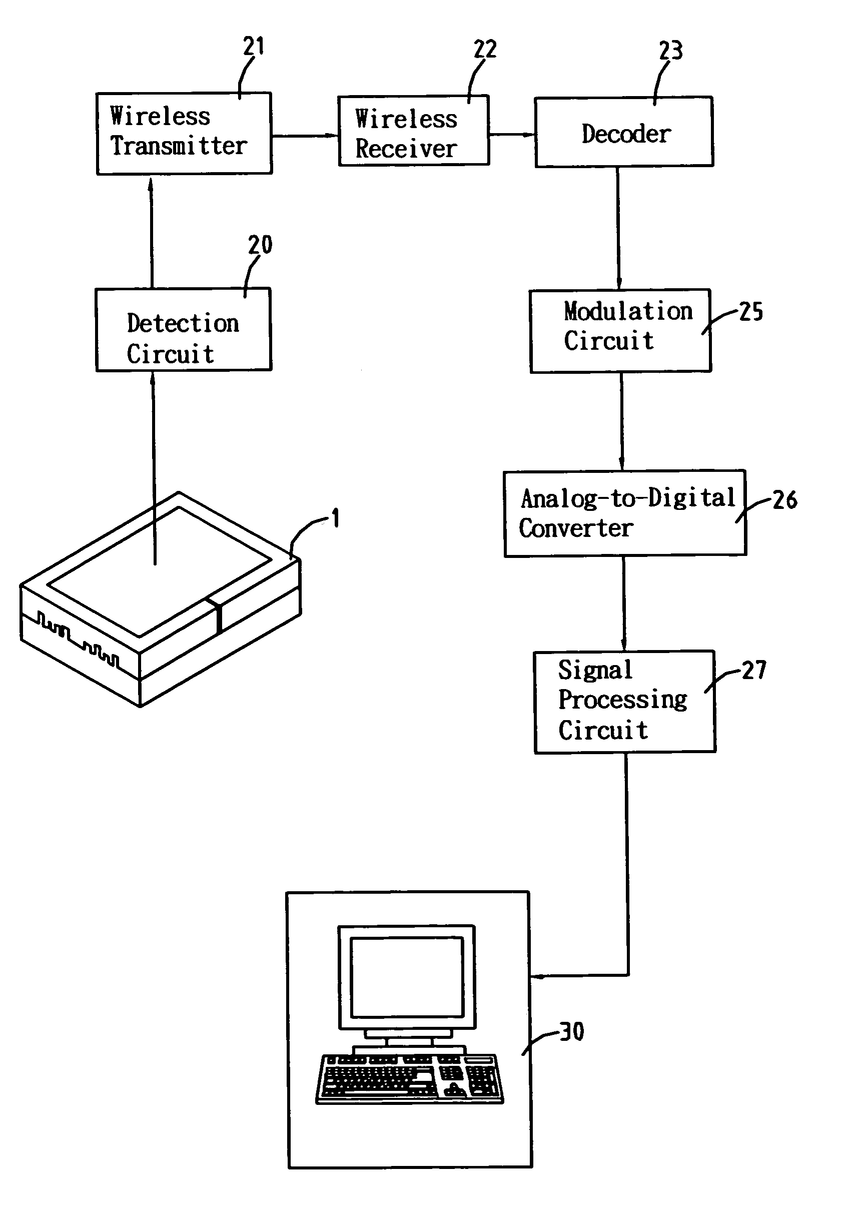
"The present invention provides a nano-imprint system with a detection device embedded in the mold for monitoring deformation during the imprinting process. The detection device detects changes in capacitance caused by the deformation of the mold and sends a signal to an external monitoring device for real-time display and analysis. The system can automatically shut down if abnormal conditions are detected. The external monitoring device can display or convert the capacitance data into a corresponding amount of mold deformation for on-line determination of shut-down of the system. The invention allows for immediate detection and direct display of mold deformation, providing an automatic quality control means."

Problems solved by technology

During the imprinting process, an external force, such as a reaction of a work, acts upon the mold and causes deformation of the mold, resulting in change of the distance between the metal film electrodes and thus variation of the capacitance of the capacitor.

Method used


Image

  • Nano-imprint system with mold deformation detector and method of monitoring the same
  • Nano-imprint system with mold deformation detector and method of monitoring the same
  • Nano-imprint system with mold deformation detector and method of monitoring the same

Examples


Embodiment Construction

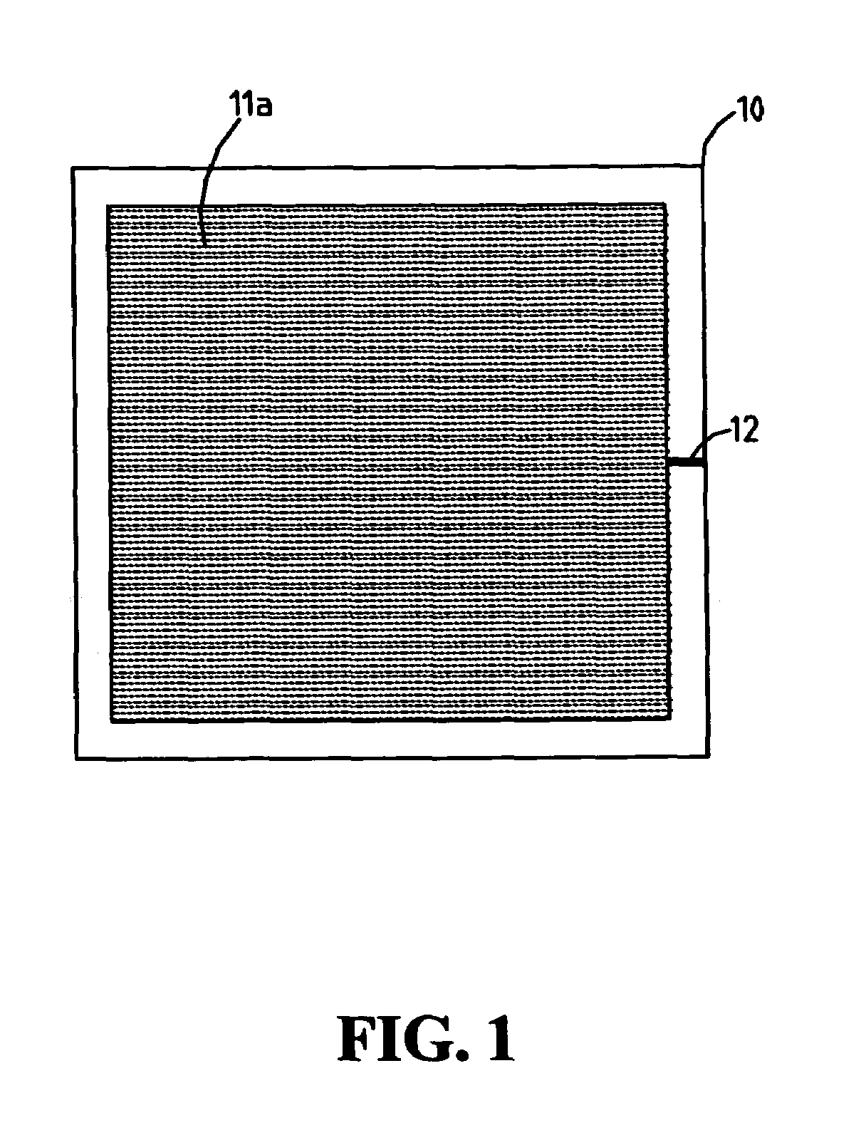
[0017]With reference to the drawings and in particular to FIG. 1, which shows a plan view of a nano-imprint mold constructed in accordance with the present invention, in which an electrostatic plate capacitor is embedded to serve as a detector for deformation of the mold, the mold of the present invention comprises a mold body 10 having a first surface facing outward, in which a first planar metal film electrode 11a is embedded. A metal lead 12 is also embedded in the mold body 10 and is electrically connected to the first metal film electrode 11a. In accordance with the present invention, both the first metal film electrode 11a and the metal lead 12 are formed by silicon micromachining technique on the mold body 10 whereby the first metal film electrode 11 and the metal lead 12 are completely integrated with the mold body 10.

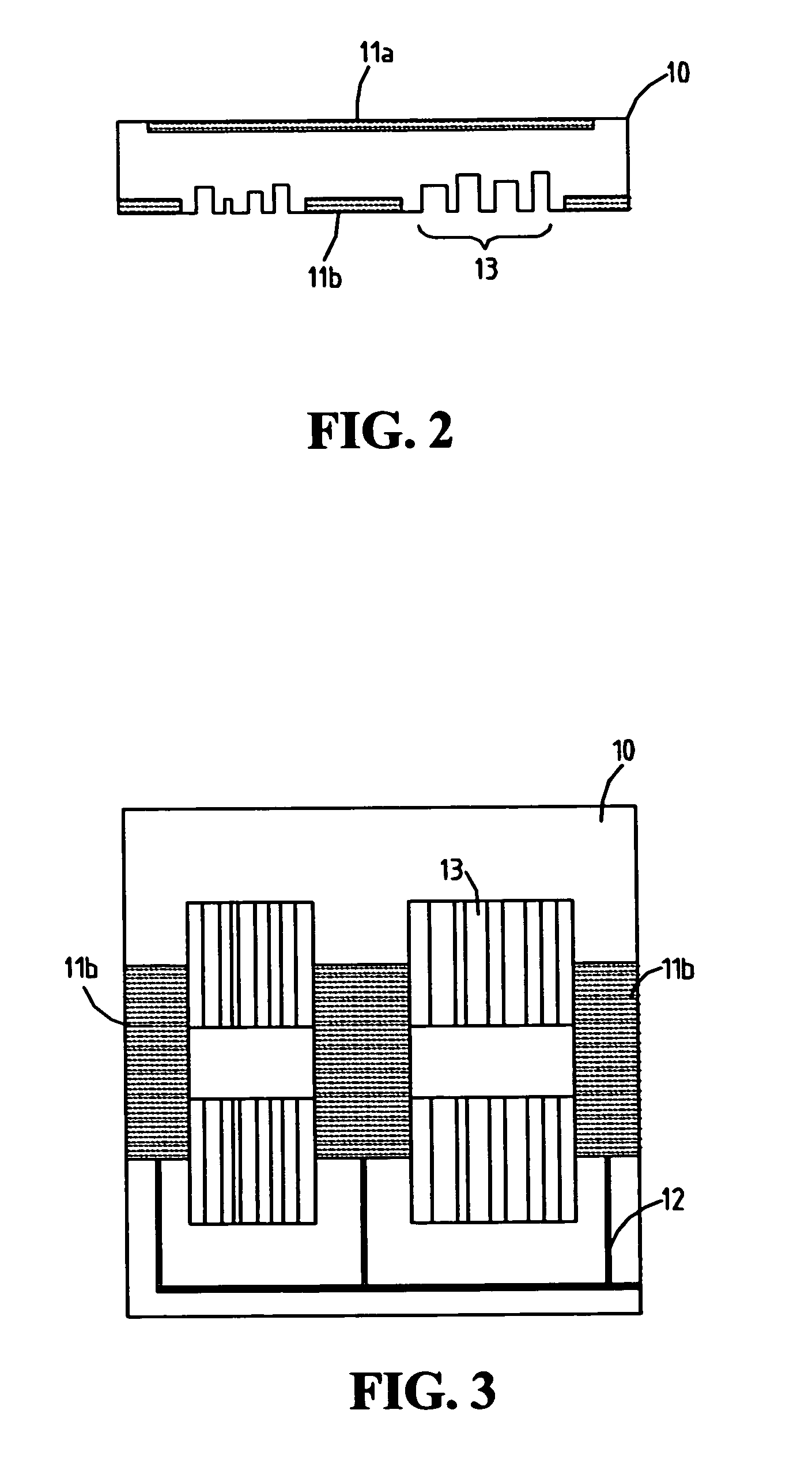
[0018]Also referring to FIGS. 2 and 3, which show a side elevational view and a bottom view of the nano-imprint mold of the present invention, respectively, a ...


PUM

PropertyMeasurementUnit
distanceaaaaaaaaaa
capacitanceaaaaaaaaaa
densityaaaaaaaaaa

Abstract

A system for nano-imprint with mold deformation detector is disclosed for real-time monitoring of the deformation of the mold. An electrostatic plate capacitor is embedded in the mold, serving as the deformation detector. The capacitor includes two opposite metal film electrodes formed by silicon micromachining technique on opposite surfaces of the mold and connected by a metal lead. During imprinting, the mold is acted upon by an external force and deformation occurs, which induces change of distance between the metal film electrodes and thus variation of the capacitance of the capacitor. The amount of deformation of the mold can then be assessed by comparing the capacitance with a reference. Thus, real-time detection and monitoring of the deformation of the nano-imprint mold is realized. Also disclosed is a method for carrying out the real-time monitoring of the deformation of the mold.

Description

FIELD OF THE INVENTION[0001]The present invention relates generally to a nano-imprint system incorporating mold deformation detection, and in particular to a nano-imprint system comprising a mold in which an electrostatic plate capacitor is embedded to function as deformation detector whereby real-time detection and monitoring of the deformation of the mold can be realized.BACKGROUND OF THE INVENTION[0002]With the advent of the nano-technology, the need of nano-structures of atom-level precision is dramatically increased. Thus, a variety of nano-imprinting techniques are developed, such as micro-contact printing, scanning probe-based techniques and nano-imprint lithography. Among these techniques, the nano-imprint lithography allows for repeated printing with one single mold that is obtained with one single lithography step. The nano-imprint lithography is thus one of the most promising techniques for nano-imprinting, having the advantages of low cost and high yield with wild applic...

Claims


Application Information

Patent Timeline
Patent Type & Authority Patents(United States)
IPC IPC(8): B29C43/58B29C45/76B29C37/00B29C43/02G01R29/22
CPCB29C37/005B29C43/003B29C43/021B29C43/58B82Y10/00B82Y40/00G03F7/0002B29C2043/025Y10S977/887B29C2059/023B29C2043/5825
Inventor HOCHENG, HONGNIEN, CHIN CHUNG
Owner NATIONAL TSING HUA UNIVERSITY
Learn More