Integrated circuit and method for testing memory on the integrated circuit

a technology of integrated circuits and integrated circuits, applied in the direction of static storage, instruments, etc., can solve the problems of bringing its own testing problems, time spent in manufacturing testing grows exponentially, and test vector style tests are not suitable for verifying embedded memory arrays

Active Publication Date: 2007-12-11
BLUE SKY MEDICAL GROUP +1
View PDF4 Cites 9 Cited by
  • Summary
  • Abstract
  • Description
  • Claims
  • Application Information

AI Technical Summary

Benefits of technology

[0013]This mechanism of the present invention is applicable to a number of programming operations of the memory test controller. For example, the sequence of test events may involve the performance of a particular test procedure on a particular sequence of memory units within the integrated circuit, the test procedure being executed on each memory unit in turn. In such instances, each piece of event defining information received during a single programming operation will identify a particular memory unit to which the test procedure is to be applied. This hence avoids the need to initiate a separate programming operation for each separate memory unit to which the test procedure is to be applied.
[0014]In an alternative embodiment, each test event is a test algorithm and the technique of the present invention is used to program a sequence of such test algorithms into the memory test controller. In that instance, each piece of event defining information defines a particular test algorithm. By such an approach, a single programming operation can be used to program in a sequence of test algorithms to be executed on a memory unit of the integrated circuit, and hence avoids the need for a separate programming operation to be performed after each test algorithm is executed, in order to load in the next test algorithm of the desired sequence.
[0019]It should be noted that in such embodiments not all of the available registers for the algorithm defining information need to be programmed if fewer than the maximum number of test algorithms are needed. This is due to the fact that the algorithm defining information in any particular register is ignored if the corresponding valid bit is not set during the programming operation. This saves test resources. In particular, in one embodiment the interface is a serial interface, and such an approach allows the serial shift process to be terminated when algorithm defining information defining the desired number of test algorithms has been shifted into the registers.

Problems solved by technology

Whilst embedded memory presents significant system performance and cost reduction advantages, it brings its own testing issues.
Test vector style tests are not suitable for verifying embedded memory arrays for a number of reasons.
Firstly, the time spent in the manufacturing test grows exponentially as the embedded memory die area increases, which often makes such test vector style testing too costly.
However, such an approach has the disadvantage that the algorithms programmed at the RTL stage may later turn out not to include a needed algorithm, thereby requiring redesign, or may indeed include an algorithm that isn't actually required, thereby wasting test time.
Whilst such an approach does provide some flexibility with regard to programming of test algorithms, it has been found that such an approach can significantly add to the time required to perform testing of the embedded memory, and also increases the complexity of the test procedure.
Whilst it is possible to provide an interface large enough to enable multiple embedded memories to be tested in parallel this increases the complexity and expense of the BIST controller, and even then it is still necessary to perform the load procedure for each different test algorithm to be programmed into the memory BIST controller.

Method used


Image

  • Integrated circuit and method for testing memory on the integrated circuit
  • Integrated circuit and method for testing memory on the integrated circuit
  • Integrated circuit and method for testing memory on the integrated circuit

Examples


Embodiment Construction

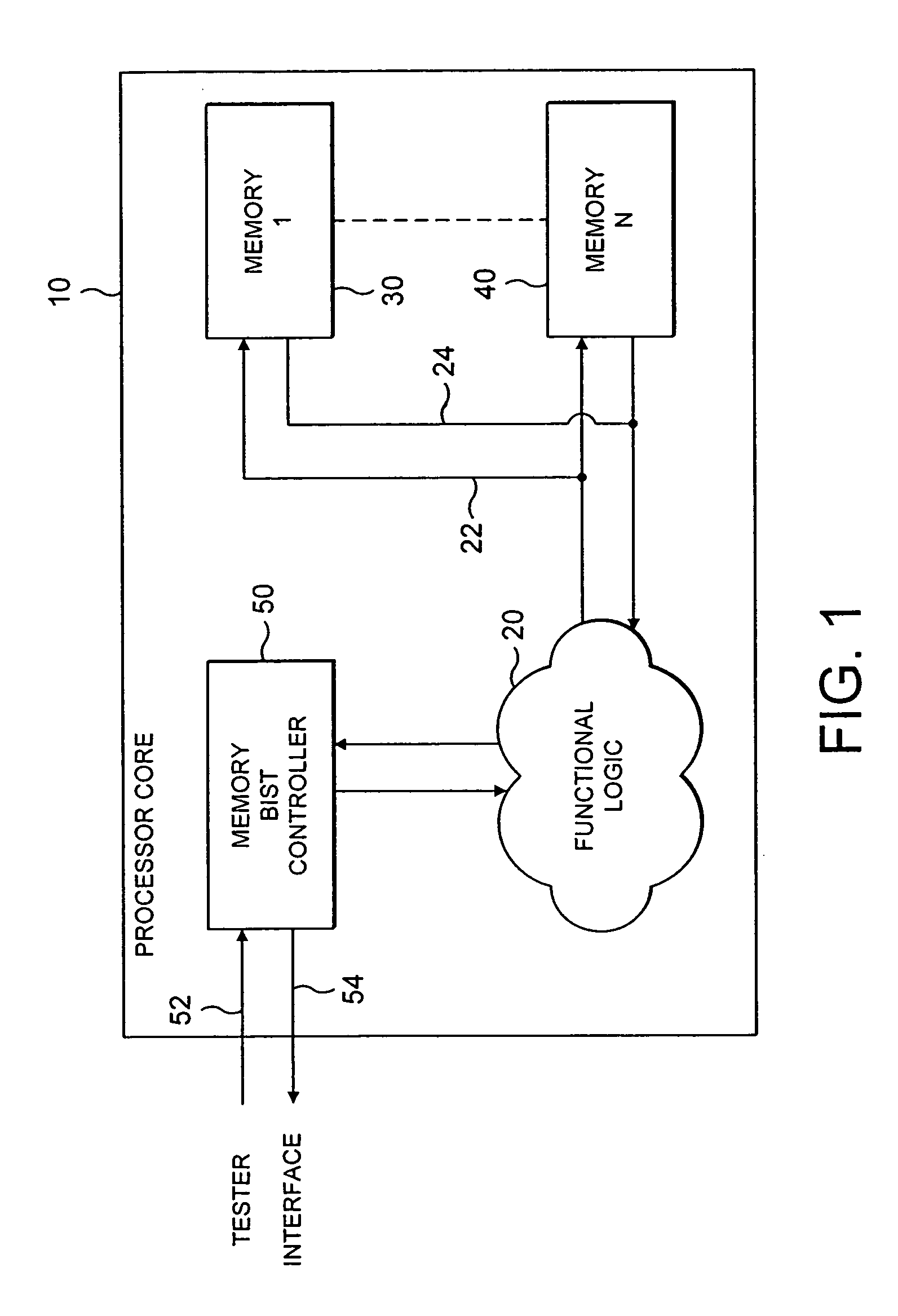
[0035]FIG. 1 is a block diagram of an integrated circuit in accordance with one embodiment of the present invention. In this particular example, the integrated circuit is a processor core. However, it will be appreciated that in other embodiments the integrated circuit may be of a different form, for example a System-on-Chip (SoC). The processor core 10 includes functional logic 20 which is coupled via a bus infrastructure 22, 24 with a number of memory devices 30, 40. The functional logic 20 will be arranged to perform a number of data processing operations, during which data will typically be written to one or more of the memory units 30, 40 and / or read from one or more of the memory units 30, 40.

[0036]The memory units 30, 40 may take a variety of forms, but in one embodiment may include caches and / or other types of embedded memory, for example Tightly Coupled Memory (TCM).

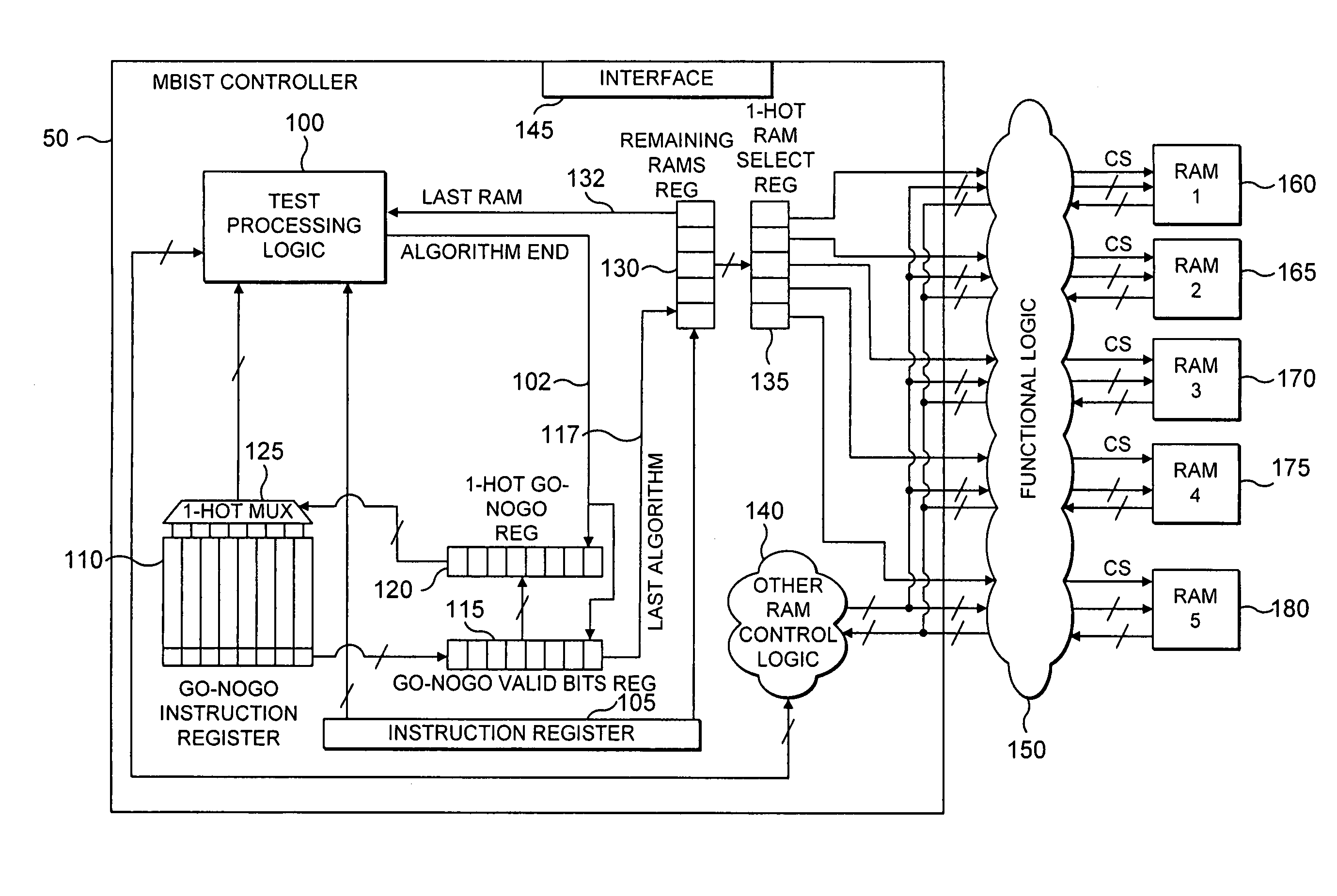
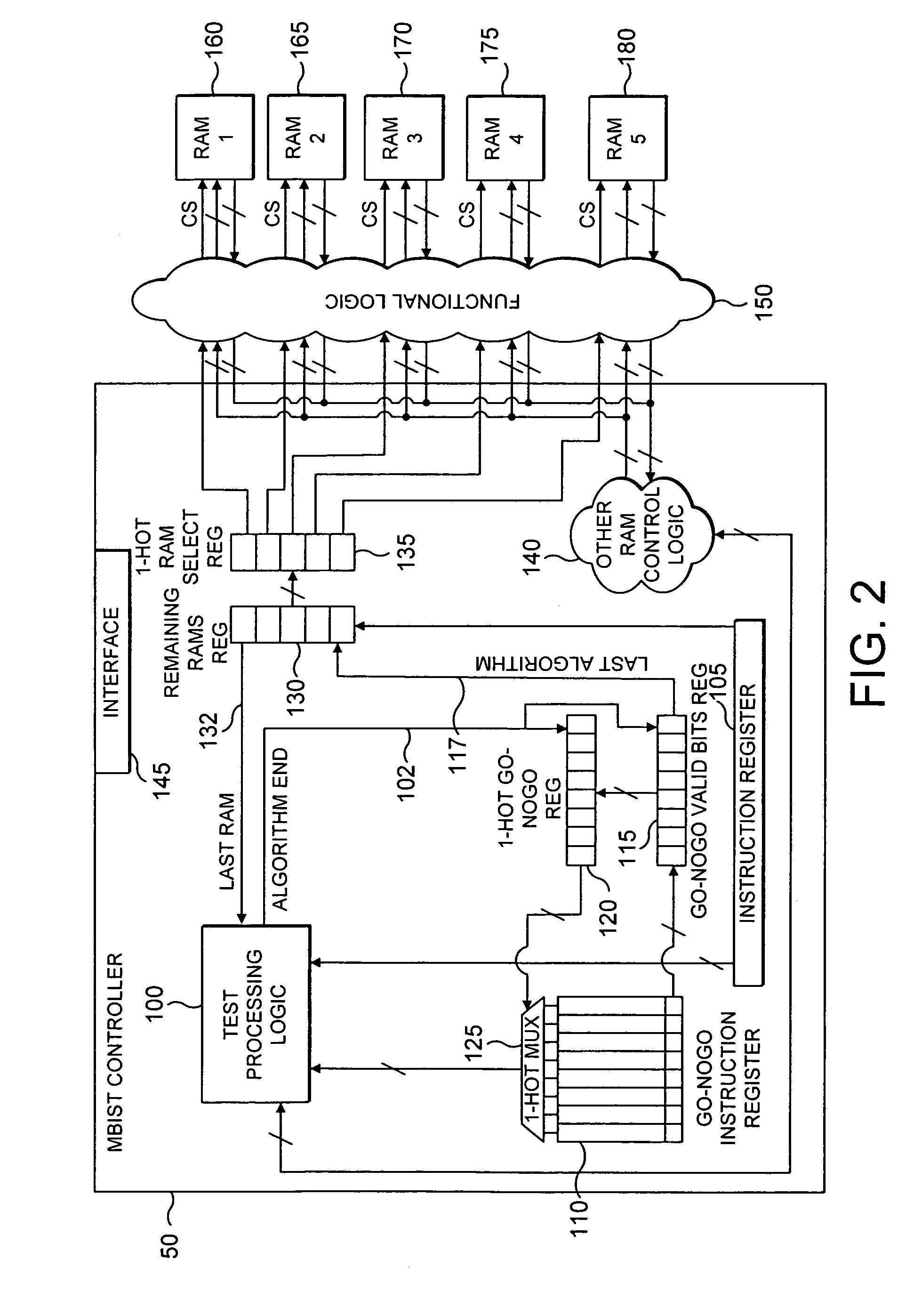
[0037]Also provided within the processor core 10 is a memory BIST controller 50 which is operable to execute ...


PUM


Abstract

An integrated circuit and method for testing memory on that integrated circuit includes processing logic operable to perform data processing operations on data, and a number of memory units operable to store data for access by the processing logic. A memory test controller is also provided for executing test events in order to seek to detect any memory defects in the number of memory units. The controller includes a storage operable to store event defining information for each of a plurality of test events forming a sequence of test events to be executed, and an interface which, during a single programming operation, receives the event defining information for each of the plurality of test events and causes that event defining information to be stored in the storage. Event processing logic within the controller is then operable, following the single programming operation, to execute the sequence of test events.

Description

BACKGROUND OF THE INVENTION[0001]1. Field of the Invention[0002]The present invention relates to an integrated circuit and method for testing memory on the integrated circuit.[0003]2. Description of the Prior Art[0004]It is becoming more and more common for integrated circuits to include embedded memory to allow rapid access to data by processing logic provided on the integrated circuit. As the use of embedded memory continues to increase, thorough testing and defect diagnosis has become a key requirement to ensure product quality and enhance product yield. Whilst embedded memory presents significant system performance and cost reduction advantages, it brings its own testing issues. Test vector style tests are not suitable for verifying embedded memory arrays for a number of reasons. Firstly, the time spent in the manufacturing test grows exponentially as the embedded memory die area increases, which often makes such test vector style testing too costly. Furthermore, it is sometimes...

Claims


Application Information

Patent Timeline
Patent Type & Authority Patents(United States)
IPC IPC(8): G11C29/00
CPCG11C29/16G11C29/26G11C29/48G11C2029/3602G11C2029/0401
Inventor SLOBODNIK, RICHARDHUGHES, PAUL STANLEYFREDERICK, FRANK DAVIDBACKLUND, BRANDON MICHAEL
Owner BLUE SKY MEDICAL GROUP
Why Eureka
Try Eureka