Ferromagnetic-semiconductor spin polarizer of electrons in nonmagnetic semiconductors

a magnetic-semiconductor, electron-spin polarizer technology, applied in the field of spintronics, can solve the problems of schottky barrier, impossible tunneling of electrons, and all attempts to achieve higher spin polarization

Inactive Publication Date: 2007-12-18
NEW PHYSICS DEVICES
View PDF1 Cites 2 Cited by
  • Summary
  • Abstract
  • Description
  • Claims
  • Application Information

AI Technical Summary

Problems solved by technology

Thus far, all of the attempts to achieve higher spin polarization have faced fundamental difficulties.
The principal difficulty of the spin injection from a ferromagnetic (FM) into a nonmagnetic semiconductor is that a potential barrier (Schottky barrier) always arises in the semiconductor near the metal-semiconductor interface.
As will be described below, the Schottky barrier forms in such a way that the junction is very wide, which makes tunneling of electrons practically impossible.
Realization of an efficient spin polarization in nonmagnetic semiconductors (NS) due to such a thermoemission current is problematic for several reasons.
Thus, the effective spin injection in the conventional FM-S Schottky junction 100 is impossible for all practical purposes.
Moreover, a fundamental problem for quantum computing is to obtain an electron spin polarization in nonmagnetic semiconductors (NS) of P.sub.n=100% at very low temperatures, such as, T<1.degree. K.

Method used


Image

  • Ferromagnetic-semiconductor spin polarizer of electrons in nonmagnetic semiconductors
  • Ferromagnetic-semiconductor spin polarizer of electrons in nonmagnetic semiconductors
  • Ferromagnetic-semiconductor spin polarizer of electrons in nonmagnetic semiconductors

Examples


Embodiment Construction

[0054]Several embodiments of the present invention will now be described in detail with reference to the annexed drawings. In the following description, detailed descriptions of known functions and configurations incorporated herein have been omitted for conciseness and clarity.

[0055]For simplicity and illustrative purposes, the principles of the present invention are described by referring mainly to exemplary embodiments thereof. In the following description, numerous specific details are set forth in order to provide a thorough understanding of the present invention. Those with skill in the art will recognize that various changes and modifications can be made to the examples provided herein without departing from the scope and spirit of the invention.

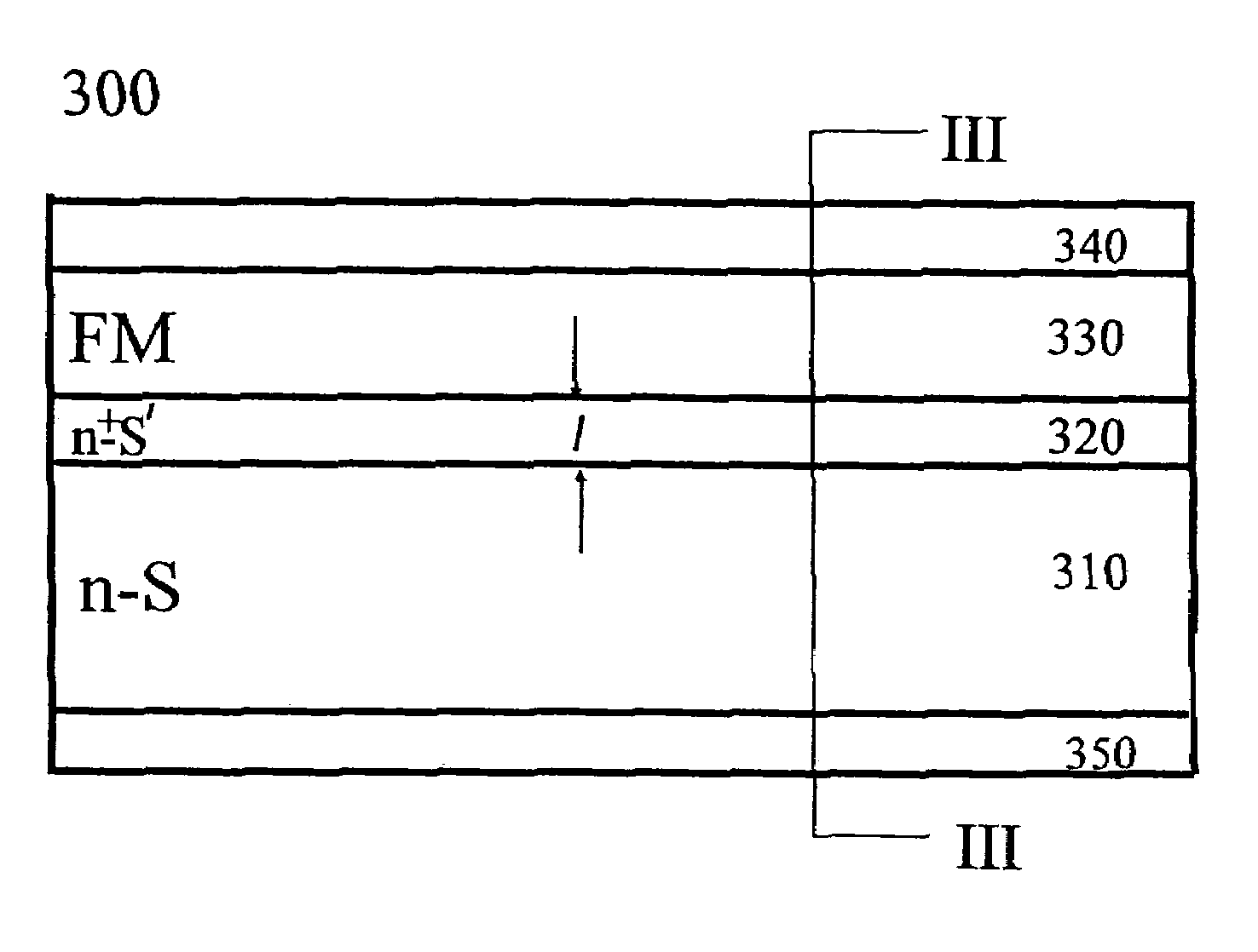
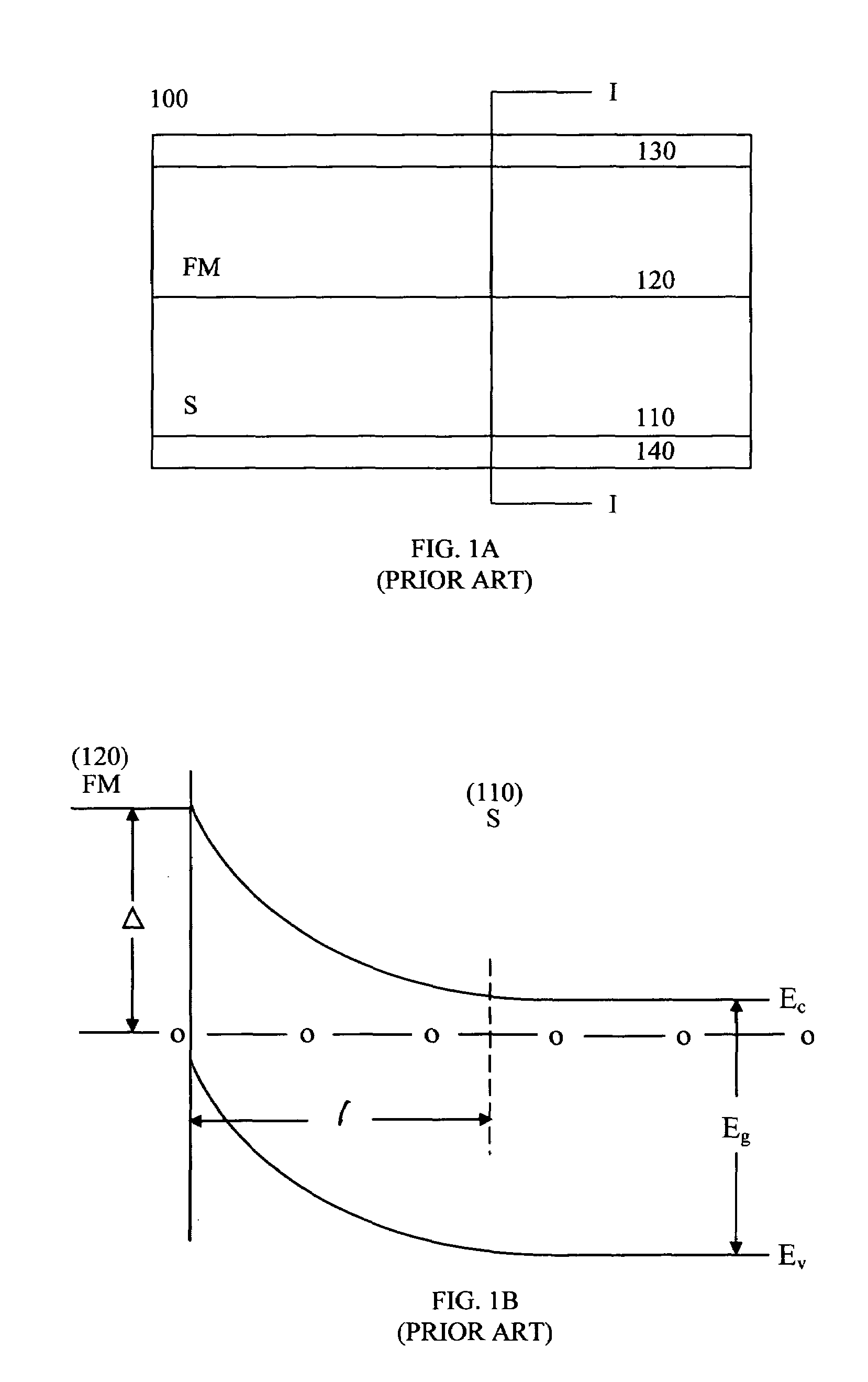
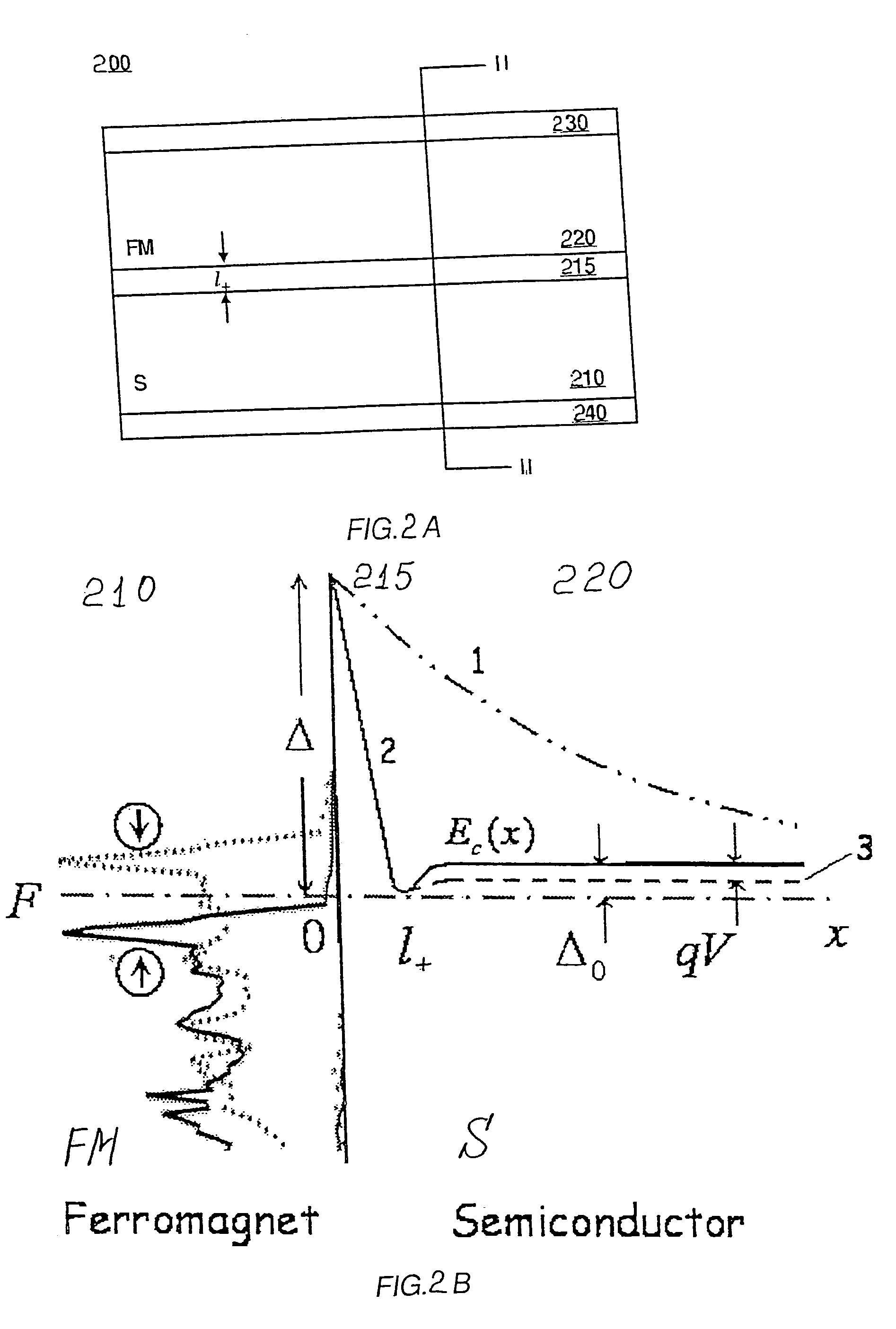
[0056]The exemplary embodiments of the present invention are a spin polarizer that in the general case, can contain a ferromagnetic-semiconductor (FM-S) junction ensuring a spin polarization of current, PJ, near a boundary with a nonm...


PUM


Abstract

An efficient spin polarizer in nonmagnetic semiconductors is provided. Previous spin injection devices suffered from very low efficiency (less than 35%) into semiconductors. An efficient spin polarizer is provided which is based on ferromagnetic-semiconductor heterostructures and ensures spin polarization of electrons in nonmagnetic semiconductors close to 100% near the ferromagnetic-semiconductor junctions at wide temperature intervals ranging from very low temperatures to room temperatures even in the case when spin polarization of electrons in the ferromagnetic layer is relatively low.

Description

BACKGROUND OF THE INVENTION[0001]1. Field of the Invention[0002]In general, the present invention relates to spintronics. In particular, the present invention relates to creating a spin polarization of virtually all of the electrons in nonmagnetic semiconductors at an arbitrary spin polarization current in ferromagnetic material and at a wide range of temperatures including room temperature.[0003]2. Description of the Related Art[0004]The entire contents of each document listed below is expressly incorporated herein by reference:[0005][1] I. Zutic, J. Fabian, and S. Das Sarma, Spintronics: Fundamentals and applications, Rev. Mod. Phys. 76, 323 (2004).[0006][2]“Semiconductor Spintronics and Quantum Computation”, edited by D. D. Awschalom, D. Loss, and N. Samarth (Springer, Berlin, 2002).[0007][3] M. Baibich, J. M. Broto, A. Fert, F. Nguyen Van Dau, F. Petroff, P. Eitenne, G. Creuzet, A. Friederich, and J. Chazelas, Phys. Rev. Lett. 61, 2472 (1988); R. E. Camley and J. Barnas, Phys. R...

Claims


Application Information

Patent Timeline
Patent Type & Authority Patents(United States)
IPC IPC(8): H01L29/76H01L29/94H01L31/062H01L31/113H01L31/119
CPCH01F1/405H01F10/193H01F1/401
Inventor OSIPOV, VIATCHESLAV V.STYLIANOS, YORGOS
Owner NEW PHYSICS DEVICES
Why Eureka
Try Eureka