
Cascode current mirror circuit operable at high speed

a current mirror circuit and current current technology, applied in the direction of instruments, amplifiers with semiconductor devices only, etc., can solve the problems of inability to design circuits that are faster than the speed of the transistor mb>22/b>, and limitations of the frequency response characteristics of the transistor

Inactive Publication Date: 2007-12-25
FUJITSU LTD
View PDF4 Cites 13 Cited by
  • Summary
  • Abstract
  • Description
  • Claims
  • Application Information

AI Technical Summary

Benefits of technology

This approach allows for the enhancement of frequency response characteristics by raising Vdsat12, enabling the cascode current mirror circuit to operate at a desired speed while maintaining operation in the saturation region for each transistor.

Problems solved by technology

As a result, the frequency response characteristics of the transistor M22 have limitations.
It is thus not possible to design a circuit that is faster than certain speed.

Method used


Image

  • Cascode current mirror circuit operable at high speed
  • Cascode current mirror circuit operable at high speed
  • Cascode current mirror circuit operable at high speed

Examples


first embodiment

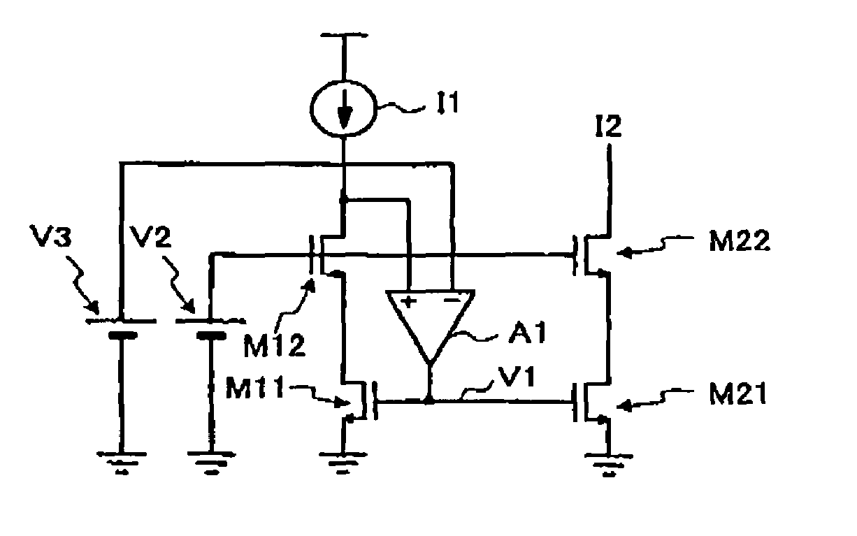
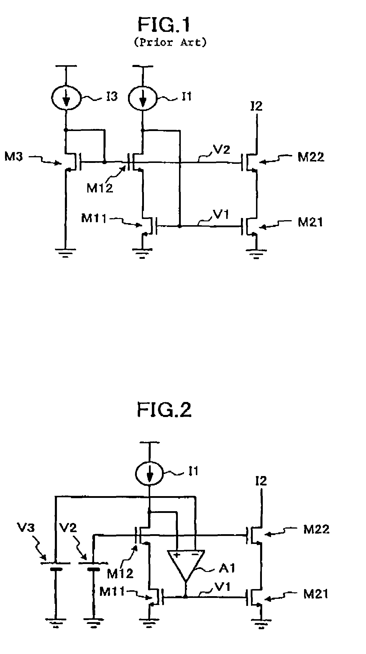
[0035]FIG. 2 is a circuit diagram showing an example of the construction of a cascode current mirror circuit according to the present invention. The cascode current mirror circuit of FIG. 2 includes a current source I1, a bias-voltage generating circuit V2, a bias-voltage generating circuit V3, NMOS transistors M11, M12, M21, and M22, and a differential amplifier A1. The output node of the differential amplifier A1 is connected to the gate node of the transistor M11, which is a source-grounded stage of the current mirror. The non-inverted input node of the differential amplifier A1 is connected to the drain of the transistor M12 which is a cascode stage. The inverted input node receives a bias voltage V3, which is necessary to make the transistor M12 at the cascode stage operate in the saturation region.

[0036]The transistors M11 and M21 have their gates connected to each other to make up a current mirror circuit. The transistors M12 and M22 also have their gates connected to each ot...

second embodiment

[0057]FIG. 6 is a circuit diagram showing an example of the construction of the cascode current mirror circuit according to the present invention. In FIG. 6, the same elements as those of FIG. 2 are referred to by the same numerals.

[0058]The cascode current mirror circuit of FIG. 6 includes the current source I1, the bias-voltage generating circuit V2, the NMOS transistors M11, M12, M21, and M22, and a current-controlled current source F1. The current-controlled current source F1 controls the amount of an electric current on the output side such that the current flowing on the output side (i.e., the side connected to the current source I1) is responsive (i.e., equal to or proportional to) the current flowing on the input side (i.e., the side connected to the drain node of the transistor M12). The current on the input side and the current on the output side may be proportional to each other with a positive proportion factor, or may be proportional to each other with a negative propor...

third embodiment

[0066]FIG. 8 is a circuit diagram showing an example of the construction of the cascode current mirror circuit according to the present invention. In FIG. 8, the same elements as those of FIG. 2 are referred to by the same numerals.

[0067]The cascode current mirror circuit of FIG. 8 includes the current source I1, the bias-voltage generating circuit V2, the NMOS transistors M11, M12, M21, and M22, and a shift-voltage generating circuit V4. The shift-voltage generating circuit V4 has its minus side connected to the gate node of the transistor M11 and its plus side connected to the drain node of the transistor M12. With this provision, a potential made by subtracting a predetermined shift voltage from the drain-node potential of the transistor M12 appears at the gate node of the transistor M11.

[0068]The transistors M11 and M21 have their gates connected to each other to make up a current mirror circuit. The transistors M12 and M22 also have their gates connected to each other to make u...


PUM


Abstract

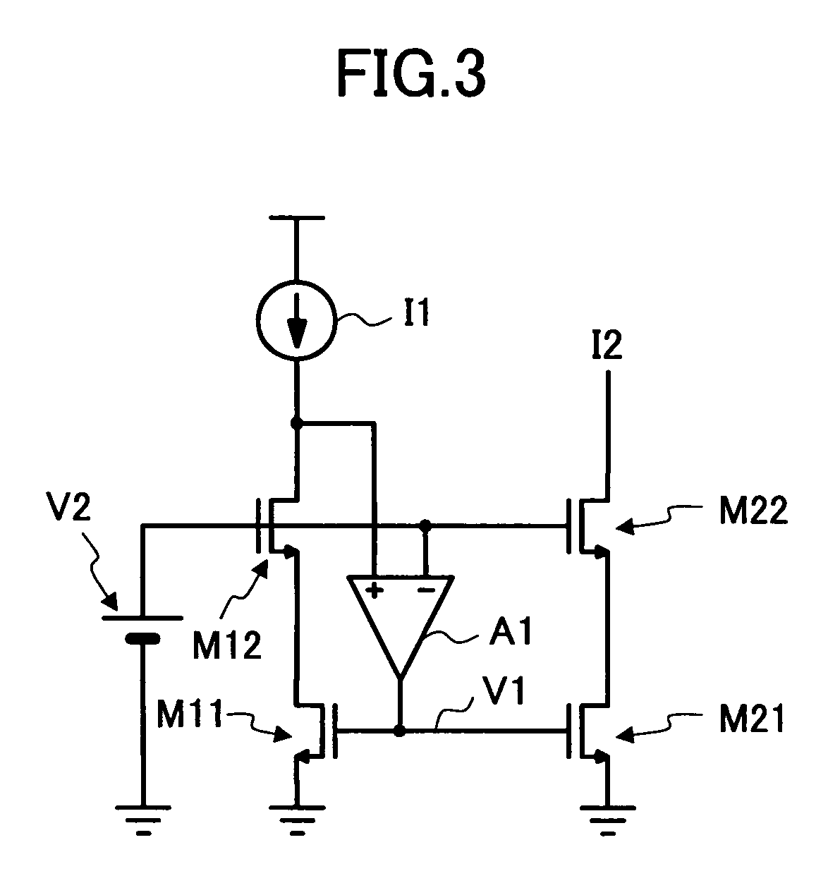
A current mirror circuit includes a first transistor having a source node connected to a reference potential, a second transistor having a source node coupled to a drain node of the first transistor and a gate node connected to a first predetermined potential, an inverted amplification circuit having a non-inverted input node coupled to a drain node of the second transistor, an inverted input node coupled to a second predetermined potential, and an output node coupled to a gate node of the first transistor, a third transistor having a gate node connected to a potential substantially equal to a potential of the gate node of the first transistor, and a fourth transistor having a gate node connected to a potential substantially equal to a potential of the gate node of the second transistor.

Description

BACKGROUND OF THE INVENTION[0001]1. Field of the Invention[0002]The present invention generally relates to circuits for controlling an electric current, and particularly relates to a cascode current mirror circuit.[0003]2. Description of the Related Art[0004]The cascode current mirror circuit has features such as extremely high output resistance and relatively high operation speed, and is used as an important analog circuit element. In the cascode current mirror circuit, transistors are arranged in tandem, which ends up lowering the voltage margin of the circuit. There is a circuit construction known to overcome this shortcoming and suitable for low-voltage operation (e.g., Non-patent Document 1). Such circuit construction is widely use.[0005]FIG. 1 is a circuit diagram showing an example of a related-art cascode current mirror circuit. The circuit of FIG. 1 includes a current source I1, a current source I3, and NMOS transistors M11, M12, M21, M22, and M3, In the following descripti...

Claims


Application Information

Patent Timeline
Patent Type & Authority Patents(United States)
IPC IPC(8): G05F3/02
CPCG05F3/262
Inventor KUDO, MASAHIRO
Owner FUJITSU LTD
Learn More