Power amplifier having a cascode current-mirror self-bias boosting circuit

A power amplifier, bias circuit technology, applied in power amplifiers, amplifiers, improving amplifiers to reduce temperature/power supply voltage changes, etc., can solve problems such as complex circuits, and achieve the effect of economic structure

Inactive Publication Date: 2004-11-24
KONINKLIJKE PHILIPS ELECTRONICS NV
View PDF6 Cites 10 Cited by
  • Summary
  • Abstract
  • Description
  • Claims
  • Application Information

AI Technical Summary

Problems solved by technology

Although this scheme is able to achieve high power-increased efficiency while maintaining linearity

Method used


Image

  • Power amplifier having a cascode current-mirror self-bias boosting circuit
  • Power amplifier having a cascode current-mirror self-bias boosting circuit
  • Power amplifier having a cascode current-mirror self-bias boosting circuit

Examples


Embodiment Construction

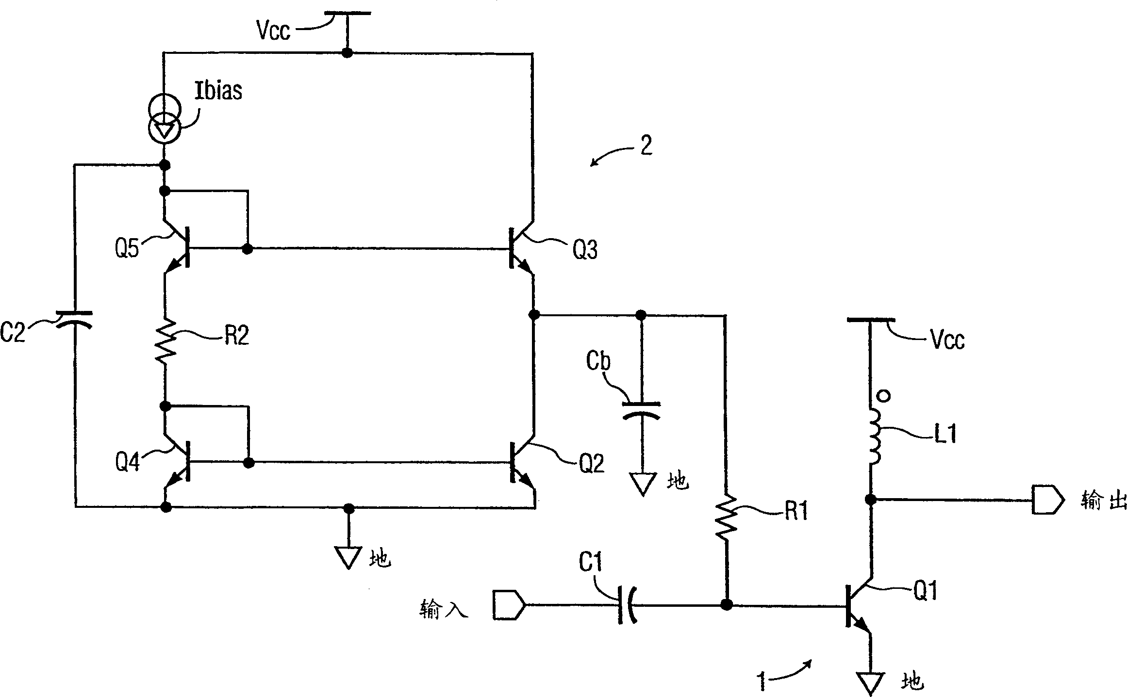
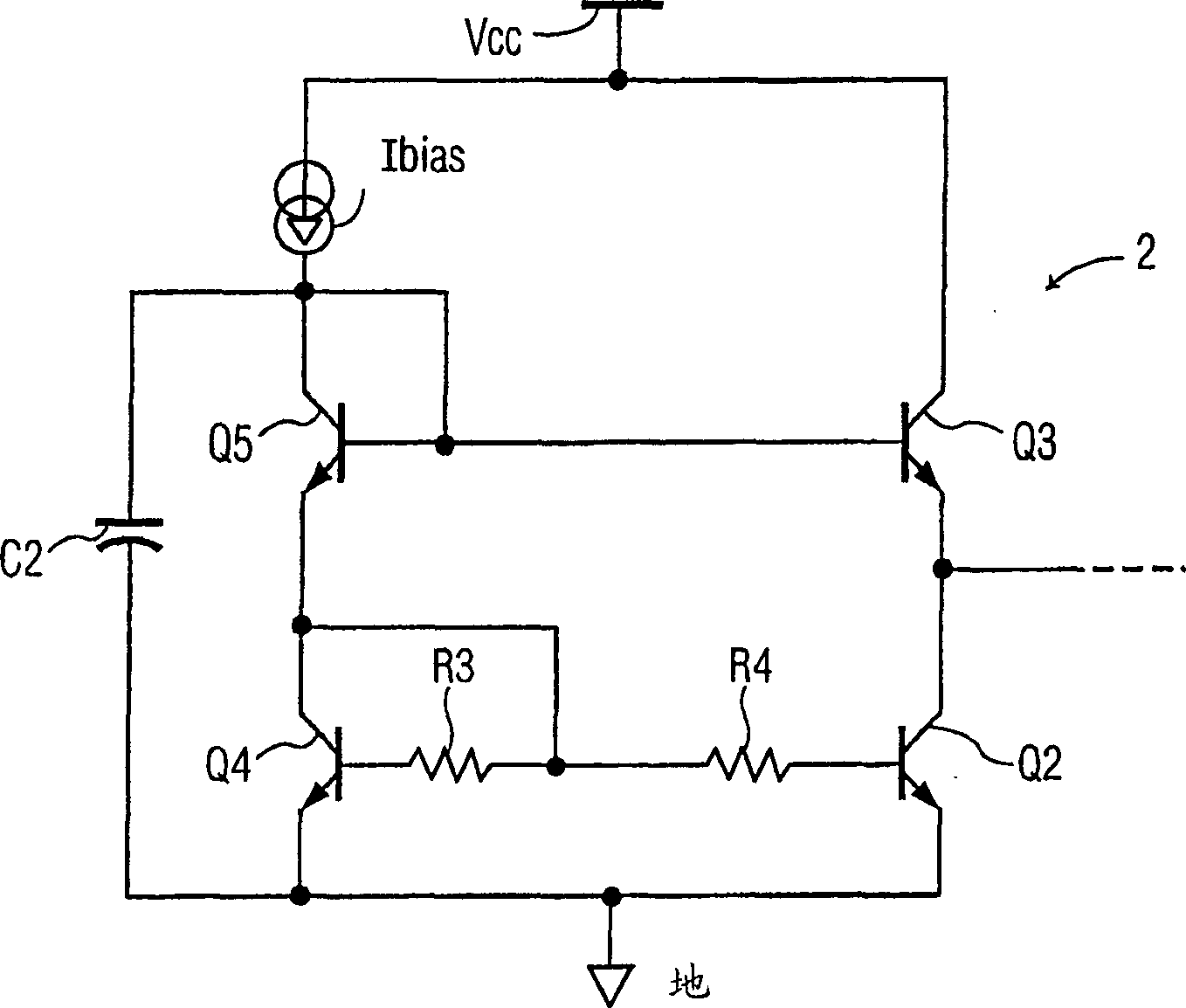
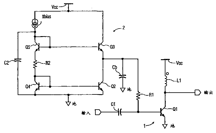
[0017] Attached figure 1 A simplified schematic diagram of the power amplifier circuit 1 is shown in . The amplifier circuit includes an amplifying transistor Q1 and a dc bias circuit 2 coupled to the base of the amplifying transistor Q1 through a resistor R1. The bias circuit 2 includes output bipolar transistors Q2 and Q3 coupled in series between Vcc and a common terminal (ground), the common point of the transistors being coupled to the common terminal via a capacitor Cb and to the transistor Q1 via a resistor R1 base. The basic circuit configuration is completed by an input coupling capacitor C1 for coupling the input signal to the base of amplifying transistor Q1, which is connected in a common-emitter configuration and coupled between Vcc and ground through an inductor L1. The output of the power amplifier circuit 1 is taken from the collector of the transistor Q1.

[0018] In conjunction with the circuit shown, it will be appreciated that although for purposes of il...


PUM


Abstract

A power amplifier circuit includes an amplifying transistor and a dc bias circuit for biasing the amplifier transistor to obtain a conduction angle of at least about 180 DEG . The dc bias circuit includes a self-bias boosting circuit which has a cascode current-mirror circuit having an output coupled to a control terminal of the amplifying transistor by a resistor, and a capacitor coupled from the cascode current-mirror circuit to a common terminal. The value of the capacitor can be selected to obtain the desired amount of self-bias boosting.

Description

Background of the invention [0001] The present invention relates to the field of transistor amplifier circuits, and more particularly, to a power amplifier circuit with a cascode current mirror self-bias boost circuit. [0002] This general-purpose type of amplifier is mostly used in high-frequency RF amplifiers, as well as in audio amplifiers and other applications. In order to obtain a linear input-output relationship and high operating efficiency, such amplifiers are usually operated with a conduction angle of about 180° (Class B), or a slightly larger conduction angle (Class AB) to avoid crossover distortion . [0003] Typically, such amplifiers require a dc bias circuit to establish a quiescent bias current in the amplifier circuit to ensure operation in Class B or Class AB mode. In the prior art, the bias is usually provided by a fixed current source, as shown in U.S. Patent No. 5,844,443, or by an external power supply, which can be set to a desired constant value to ...

Claims


Application Information

Patent Timeline
IPC IPC(8): H03F1/30H03F3/21
CPCH03F1/302H03F2200/108H03F2200/18H03F1/30
Inventor S·罗
Owner KONINKLIJKE PHILIPS ELECTRONICS NV
Why Eureka
Try Eureka