Biasing scheme for low-voltage MOS cascode current mirrors

a cascode current mirror and biasing scheme technology, applied in the field of semiconductor circuits, can solve the problems of output voltage swing, limited output voltage range for which the output resistance remains high, and loss of voltage range further compounded

Active Publication Date: 2009-12-29
TEXAS INSTR INC
View PDF5 Cites 13 Cited by
  • Summary
  • Abstract
  • Description
  • Claims
  • Application Information

AI Technical Summary

Problems solved by technology

An undesirable side effect of cascading, however, is that output voltage swing (range of output voltage for which the output resistance remains high) becomes limited due to the need to maintain additional series-connected devices in their active (e.g., saturated for MOS devices) operating regions.
This problem of loss of voltage range is further compounded by a trend toward lower voltage power supplies in small geometry processes.
For example, losing 1.0 V of output range can be significant, resulting in total output voltage swings of less than 1.5 V, where a 2.5 V voltage supply is involved.
The problem worsens with portable electronic devices, personal medical electronics, and wireless applications where supply voltage ranges are now typically lower than 2.5 V.
In many kinds of MOS technologies, there is no ability to directly short together the bulk terminal and the source terminal, to conveniently set the voltage of the two terminals to be the same.
These conditional variations will cause the performance of the CCCM to not mirror current accurately and vary in a way that is not solved by the prior art biasing schemes.
The prior art schemes also tend to work poorly when the cascode and mirror transistors are of different type (technology kind) transistors.
The prior art schemes also tend to be more optimal for transistors with long gate lengths (L) wherein the gate W / L ratio then may become low enough to where the transistor models are less reliable, a problem during the design phase of the circuit.
Although the output voltage Vout has improved voltage swing, the current matching suffers because the Vds voltage of Q1 and Q2 differ.

Method used


Image

  • Biasing scheme for low-voltage MOS cascode current mirrors
  • Biasing scheme for low-voltage MOS cascode current mirrors
  • Biasing scheme for low-voltage MOS cascode current mirrors

Examples


Embodiment Construction

[0024]FIGS. 1a and 1b are discussed above in the Background of the Invention section of this document and the reader is assumed familiar with the principles of that discussion.

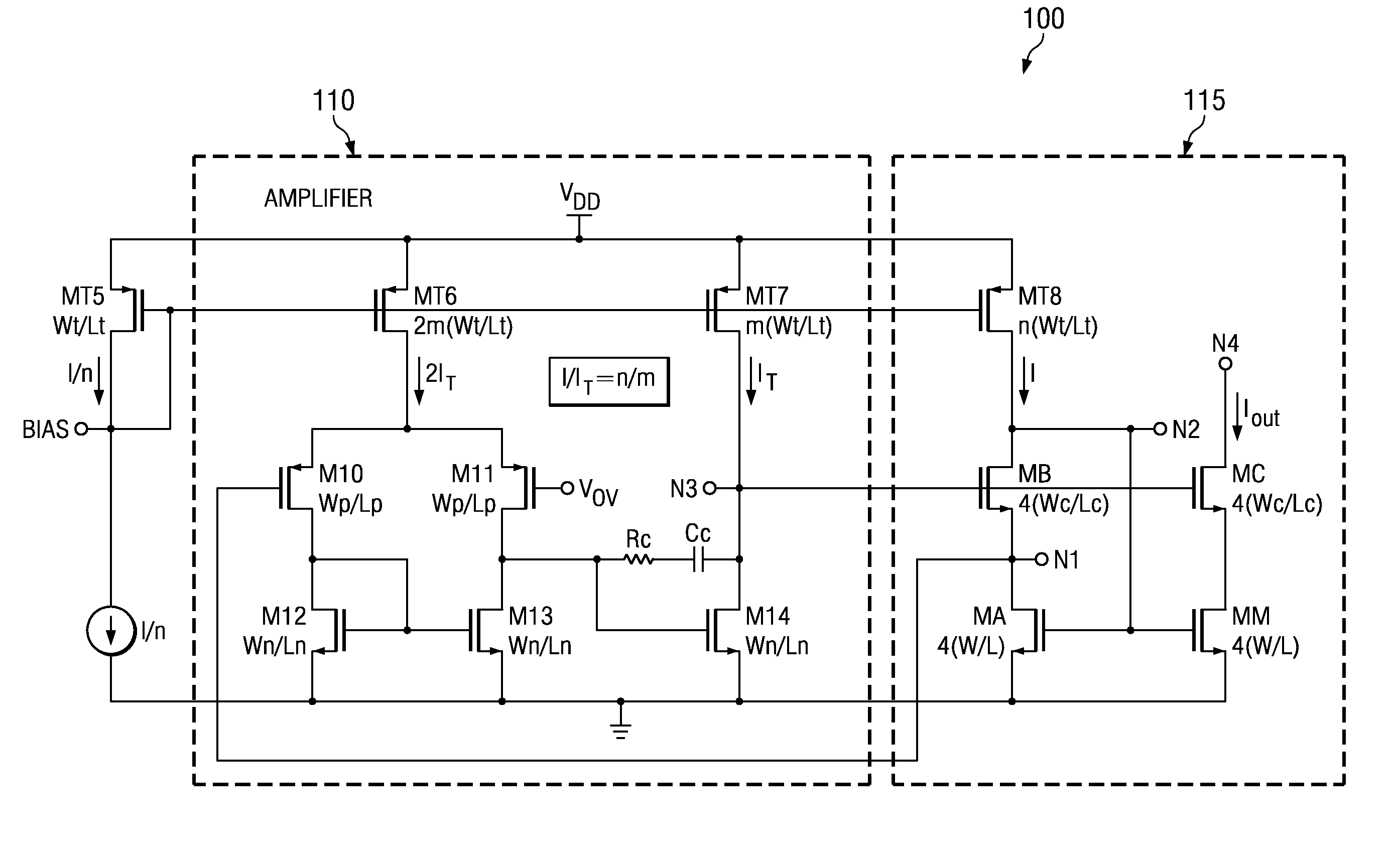
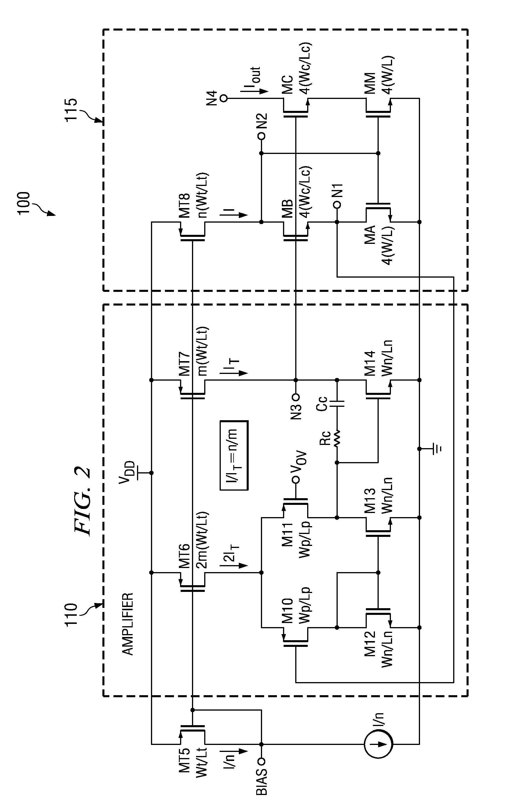
[0025]FIGS. 2 and 3 are circuit schematics illustrating a preferred embodiment of a CCCM, compound cascode current mirror, and its associated bias circuit. FIG. 2 dashed-box element 115 comprises a CCCM circuit and dashed-box element 110 comprises an amplifier with an input voltage labeled Vov. The Vov voltage is generated by the bias circuit 200 in FIG. 3.

[0026]In FIG. 2, an input current I for the CCCM is sourced by MT8's drain (node N2). CCCM has two current legs, an input leg comprising transistors (MA,MB) and an output leg (MM,MC). MA and MM are the two mirror transistors, which share the same Vgs voltage (gate-source voltage: gate nodes connected together at N2 and source nodes connected together at a voltage terminal such as ground). For accurate current mirroring, the Vds (drain-source voltage) of MA a...


PUM


Abstract

A circuit and a method for biasing a compound cascode current mirror (CCCM) that enables high-voltage swing at the output and accurate current mirroring is presented. The CCCM has mirror transistors and cascode transistors which may be of a different technology kind. The drain-source voltage Vds of the mirror transistor on the input leg of the CCCM is held at a voltage Vov that is generated by the biasing circuit; Vov is the overdrive voltage of the input mirror transistor of the CCCM and the value of Vov is maintained by the bias circuit and a feed-back amplifier such that the mirror transistor remains on the edge of its active region, over manufacture deviations and tracks even over operational conditions such as temperature and supply variations. The feed-back amplifier drives the gates of the cascode transistors and uses its feedback node to hold the Vds at Vov.

Description

CROSS-REFERENCES TO RELATED APPLICATIONS[0001]Not Applicable.STATEMENT REGARDING FEDERALLY SPONSORED RESEARCH OR DEVELOPMENT[0002]Not Applicable.FIELD OF THE INVENTION[0003]The present embodiments relate to semiconductor circuits such as on a chip (IC) or to circuits with discrete components such as on a printed circuit board (PCB) and are more particularly directed to a cascode current mirror circuit and a biasing scheme for the mirror circuit.BACKGROUND OF THE INVENTION[0004]Electronic circuits generally include current mirrors as a basic building block in order to transfer current, to provide bias current sources which may further provide bias voltage sources. Current mirrors may also exist as part of the signal path rather than the bias path, such as in current feedback amplifiers. A current mirror is a circuit which, ideally, has zero input impedance to receive an input bias current and infinite output impedance, so that current output remains a fixed function of current input ...

Claims


Application Information

Patent Timeline
Patent Type & Authority Patents(United States)
IPC IPC(8): H03F3/04
CPCG05F3/262H03F1/301H03F3/345H03F2200/91H03F2200/456H03F2200/513H03F2200/447
Inventor ARAKALI, ABHIJITHRAFEEQUE, SUNIL
Owner TEXAS INSTR INC
Why Eureka
Try Eureka