Self calibrating transmit path correction system

a transmission path correction and self-calibration technology, applied in the field of communication devices, can solve the problems of affecting the quality of modulated transmit signals, specified non-idealities, and degradation of error vector magnitude (evm), uplink bit error rate (ber), and the required transmit spectral mask performan

Active Publication Date: 2007-12-25
GOOGLE TECH HLDG LLC
View PDF9 Cites 40 Cited by
  • Summary
  • Abstract
  • Description
  • Claims
  • Application Information

AI Technical Summary

Problems solved by technology

Non-idealities, such as direct current (DC) offsets and in-phase (I) and quadrature (Q) gain and phase imbalances, in the transmit signal path of a communication device can affect the quality of the modulated transmit signal.
The specified non-idealities occur primarily due to circuit level mismatches in the analog quadrature circuitry at baseband as well as in the radio frequency (RF) and / or intermediate frequency (IF) signal paths.
These transmit path non-idealities lead to degradation in the error vector magnitude (EVM), uplink bit error rate (BER), and the required transmit spectral mask performance.
Also, in the case of 3G Wideband Code Division Multiple Access (WCDMA) transceivers, such non-idealities lead to degradation in Peak Code Domain Error (PCDE) performance.

Method used


Image

  • Self calibrating transmit path correction system
  • Self calibrating transmit path correction system
  • Self calibrating transmit path correction system

Examples


Embodiment Construction

)

[0017]As required, detailed embodiments of the present invention are disclosed herein; however, it is to be understood that the disclosed embodiments are merely exemplary of the invention, which can be embodied in various forms. Therefore, specific structural and functional details disclosed herein are not to be interpreted as limiting, but rather should be interpreted merely as a basis for the claims and as a representative basis for teaching one skilled in the art to variously employ the present invention in virtually any appropriately detailed structure. Further, the terms and phrases used herein are not intended to be limiting; but rather are intended to provide an understandable description of the invention.

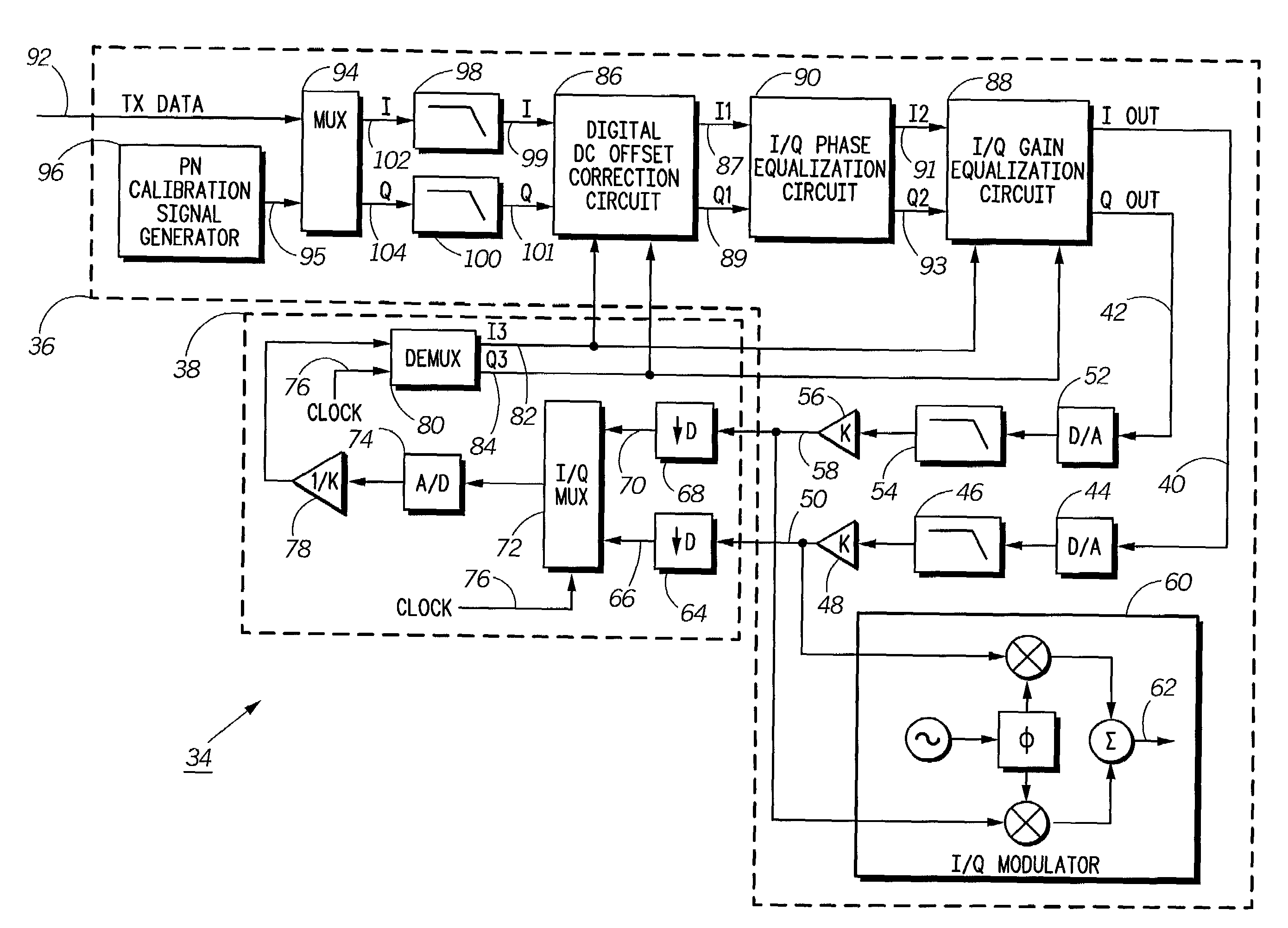
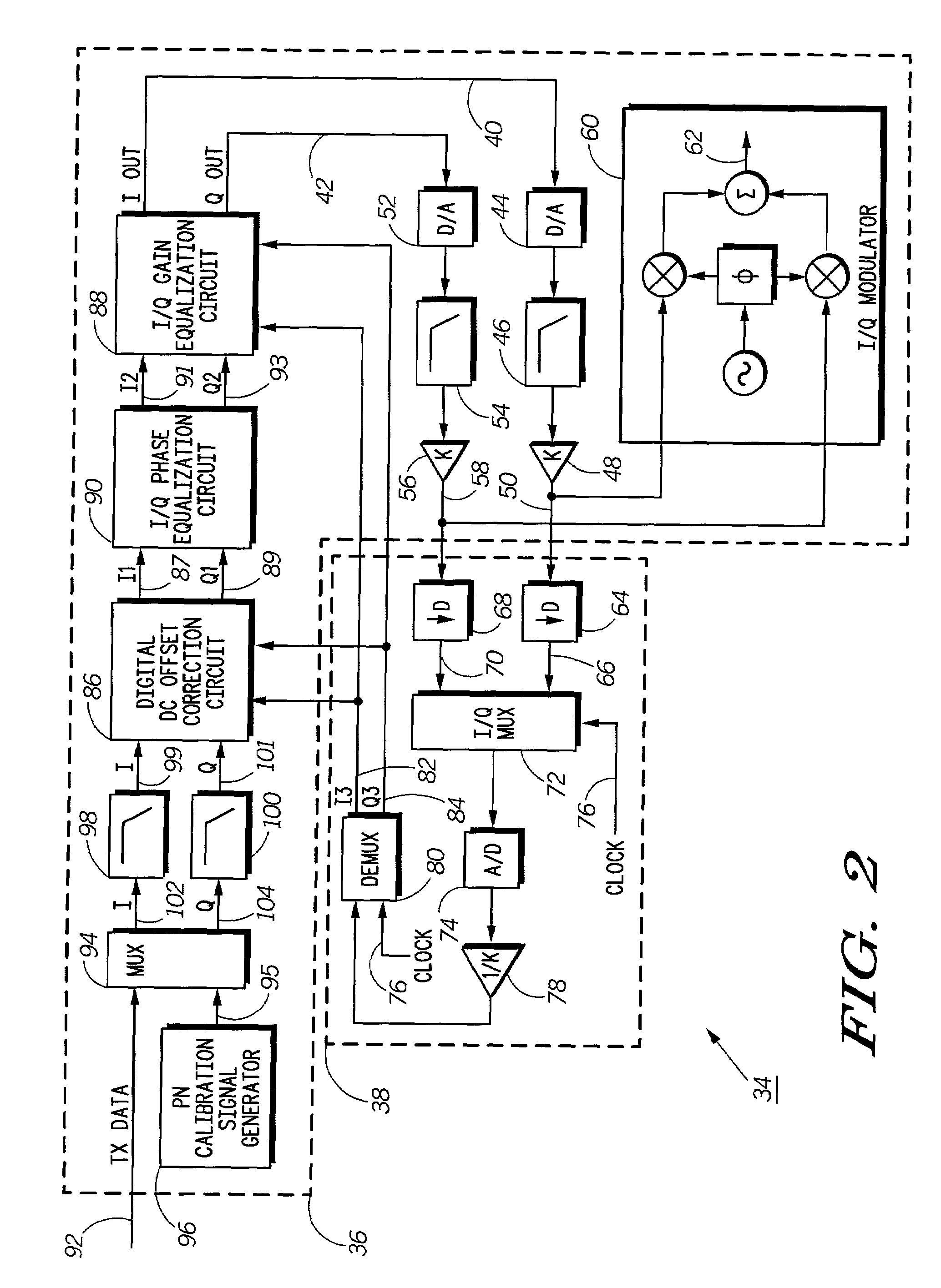
[0018]Referring to FIG. 2, a block diagram of a transmit path correction system 34 in accordance with the present invention is illustrated. The transmit path correction system 34 preferably compensates for DC offsets and I / Q gain imbalances in a closed loop manner while pro...


PUM


Abstract

A transmit path correction system (34) for compensating for digital DC offsets, I/Q gain imbalances and I/Q phase imbalances includes a mixed signal forward path (36) and a mixed signal feedback path (38). The forward pat (36), which is operable to process input data symbols to produce at least one analog output signal, preferably includes a digital DC offset correction circuit (86) for compensating for digital DC offsets in the forward path (36) using at least one digital feedback signal (82, 84), an I/Q phase equalization circuit (90) for compensating for the I/Q phase imbalances in the forward path (36), and an I/Q gain equalization circuit (88) for compensating for the I/Q gain imbalances in the forward path (36) using the digital feedback signal(s) (82, 84). The feedback pat (38) processes the analog output of the forward path (36) to produce the digital feedback signal(s) (82, 84).

Description

BACKGROUND OF THE INVENTION[0001]1. Field of the Invention[0002]This invention relates in general to communication devices and in particular to communication devices incorporating a transmit signal path correction system with self-calibration capabilities.[0003]2. Description of the Related Art[0004]Non-idealities, such as direct current (DC) offsets and in-phase (I) and quadrature (Q) gain and phase imbalances, in the transmit signal path of a communication device can affect the quality of the modulated transmit signal. The specified non-idealities occur primarily due to circuit level mismatches in the analog quadrature circuitry at baseband as well as in the radio frequency (RF) and / or intermediate frequency (IF) signal paths. These transmit path non-idealities lead to degradation in the error vector magnitude (EVM), uplink bit error rate (BER), and the required transmit spectral mask performance. Also, in the case of 3G Wideband Code Division Multiple Access (WCDMA) transceivers,...

Claims


Application Information

Patent Timeline
Patent Type & Authority Patents(United States)
IPC IPC(8): H04L27/00H04L27/04
CPCH04L27/0014H04L2027/0016
Inventor RAHMAN, MAHIBURTALWALKAR, SUMIT ANILZOCHER, ANDREW GERALD
Owner GOOGLE TECH HLDG LLC
Why Eureka
Try Eureka