

Digital offset phase-locked loop
a phase-locked loop and digital offset technology, applied in the field of phase-locked loops, can solve the problems of increasing the complexity of wireless communication protocols and demanding bandwidth utilization, high in-band noise of some traditional plls, and not being able to support the required modulation bandwidth, etc., to achieve the effect of maintaining linearity, reducing loop gain, and flexible and programmable loop filter functionality
- Summary
- Abstract
- Description
- Claims
- Application Information
AI Technical Summary
Benefits of technology
Problems solved by technology
Method used
Image

Examples
Embodiment Construction
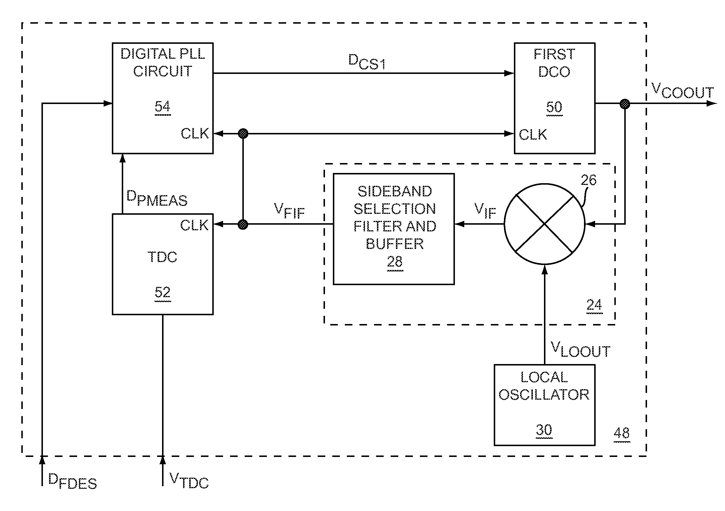
[0017]The present invention relates to a digital offset phase-locked loop (DOPLL), which may have advantages of size, simplicity, performance, design portability, or any combination thereof, compared to analog-based phase-locked loops (PLLs). The DOPLL may include a digital controlled oscillator (DCO), which provides a controllable frequency output signal based on a digital control signal, an RF mixer circuit, which provides a reduced-frequency feedback signal based on the controllable frequency output signal without reducing loop gain, a time-to-digital converter (TDC), which provides a digital feedback signal that is a time representation of the reduced-frequency feedback signal, and digital PLL circuitry, which provides the digital control signal based on the digital feedback signal and a digital setpoint signal.
[0018]Compared to analog-based PLLs, the DOPLL implements the phase detector and loop filter functions in digital logic as part of the digital PLL circuitry instead of in...
PUM
 Abstract
Description
Claims
Application Information