System on a chip for caching of data packets based on a cache miss/hit and a state of a control signal

a data packet and control signal technology, applied in the field of system on a chip, can solve the problems of packet transmission failure and having to be retransmitted, and achieve the effects of reducing the latency of a write, low latency access, and low latency to the interrup

Inactive Publication Date: 2008-01-15
AVAGO TECH INT SALES PTE LTD
View PDF47 Cites 14 Cited by
  • Summary
  • Abstract
  • Description
  • Claims
  • Application Information

AI Technical Summary

Benefits of technology

[0007]A packet processing system is described. A processor, a cache, a memory controller, and at least one packet interface circuit may be integrated into a single integrated circuit. In one implementation, the design may take advantage of the integration to form tight coupling between the processor, cache, memory controller, and packet interface circuit. For example, interrupts to the processor may be tightly coupled, with low latency to the interrupt as well as low latency access to interrupt status / reason registers. Memory coherency may be maintained among the devices, which may reduce the latency from a write by one device being visible to other devices. The memory coherency and low latency access to memory by the packet interface circuit may provide tight coupling for descriptors used to store packet data.
[0008]In one embodiment (which may be used in integrated or non-integrated systems), the packet interface circuit is configured to cause allocation in the cache of a portion of a received packet. Particularly, the portion may include bytes expected to be processed by the processors, while the remaining packet data may be stored in memory. The processors may experience cache latencies for access to the packet data, and cache pollution with data that is not accessed by the processors may be avoided.
[0009]In one embodiment (which may be used in integrated or non-integrated systems), the memory controller may be configured to selectively block memory transactions. Particularly, the memory controller may implement at least two block signals, one for the packet interface circuit and one for other devices. The block signals may be used to control the initiation of memory transactions when the memory controller's input queue is approaching fullness. Particularly, the block signal for the other devices may be asserted when the queue still has entries remaining (e.g. at about 75% fullness, although the threshold may be programmable to any level), to reduce the latency which may be experienced by read memory transactions from the packet interface circuit (for reading packet data to be transmitted on the external packet interface) when the queue is filling with transactions. In some embodiments, the failure to continuously transmit a full packet on the external packet interface may result in the packet transmission failing and having to be retransmitted. By reducing the latency, the likelihood that subsequent cache blocks of the packet are not available in the packet interface circuit when needed may be reduced.

Problems solved by technology

In some embodiments, the failure to continuously transmit a full packet on the external packet interface may result in the packet transmission failing and having to be retransmitted.

Method used


Image

  • System on a chip for caching of data packets based on a cache miss/hit and a state of a control signal
  • System on a chip for caching of data packets based on a cache miss/hit and a state of a control signal
  • System on a chip for caching of data packets based on a cache miss/hit and a state of a control signal

Examples


Embodiment Construction

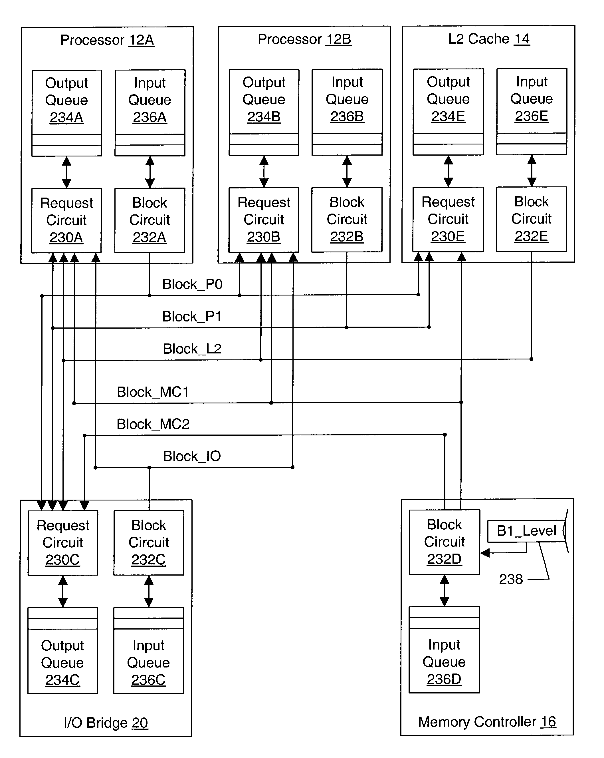
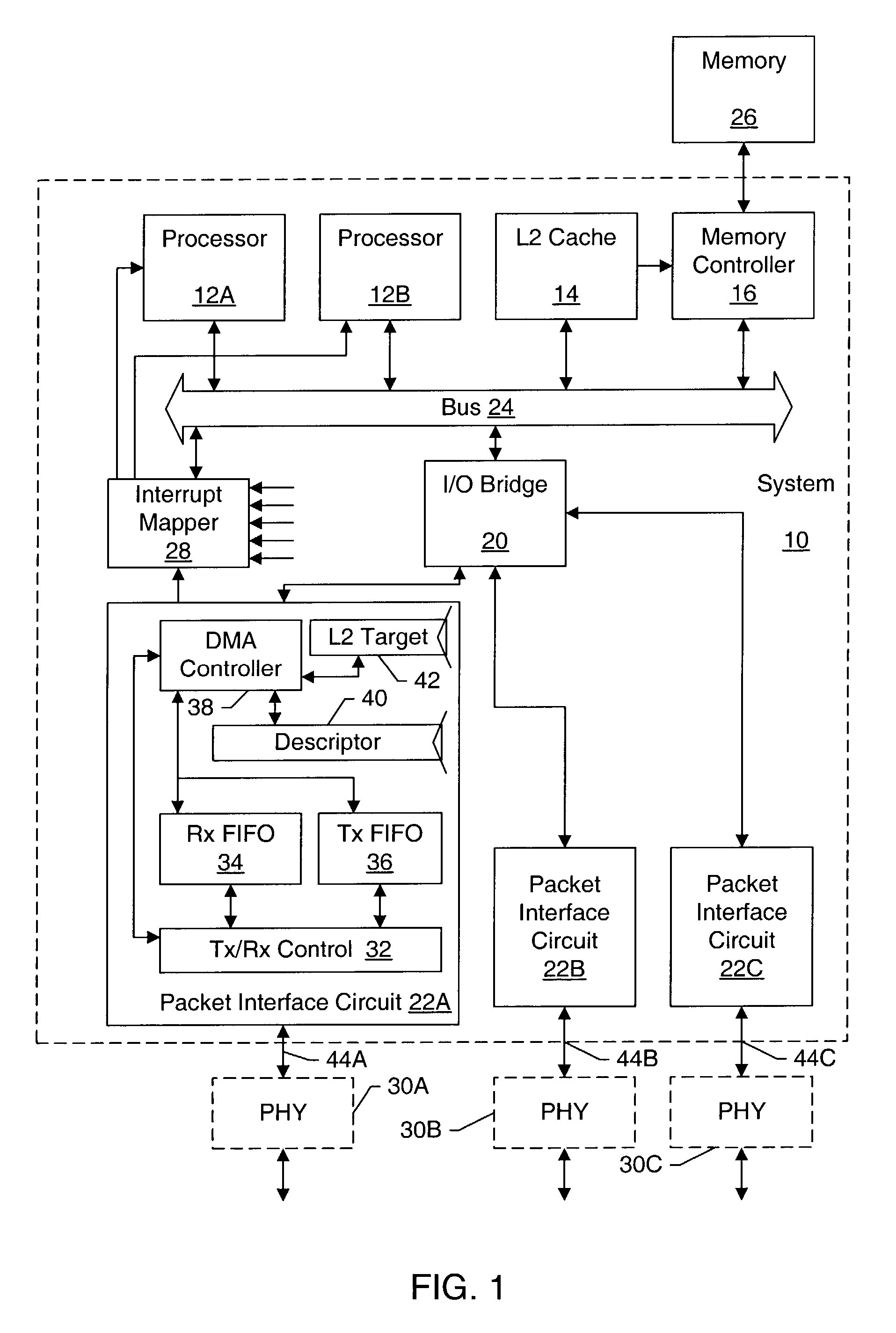
[0024]Turning now to FIG. 1, a block diagram of one embodiment of a system 10 is shown. Other embodiments are possible and contemplated. In the embodiment of FIG. 1, the system 10 includes processors 12A-12B, an L2 cache 14, a memory controller 16, an input / output (I / O) bridge 20, a set of packet interface circuits 22A-22C, and an interrupt mapper 28. The system 10 may include a bus 24 for interconnecting the various components of the system 10. As illustrated in FIG. 1, each of the processors 12A-12B, the L2 cache 14, the memory controller 16, and the I / O bridge 20 are coupled to the bus 24. Thus, each of the processors 12A-12B, the L2 cache 14, the memory controller 16, and the I / O bridge 20 may be an agent on the bus 24 for the illustrated embodiment. The interrupt controller 28 is also shown coupled to the bus 24 for communicating with the processors 12A-12B (e.g. the processors 12A-12B may read status / reasons registers in the interrupt controller 28). The I / O bridge 20 is coupl...


PUM


Abstract

A packet processing system may include a processor, a cache, a memory controller, and at least one packet interface circuit integrated into a single integrated circuit. In one embodiment (which may be used in integrated or non-integrated systems), the packet interface circuit is configured to cause allocation in the cache of a portion of a received packet. In one embodiment (which may be used in integrated or non-integrated systems), the memory controller may be configured to selectively block memory transactions. Particularly, the memory controller may implement at least two block signals, one for the packet interface circuit and one for other devices. The block signals may be used to control the initiation of memory transactions when the memory controller's input queue is approaching fullness.

Description

[0001]This application is a continuation of U.S. patent application Ser. No. 09 / 861,188, filed May 18, 2001.BACKGROUND OF THE INVENTION[0002]1. Field of the Invention[0003]This invention is related to the fields of packet processing, networking, and system on a chip.[0004]2. Description of the Related Art[0005]Networking of computer systems and other electronic devices has become more and more prevalent, at all levels of the network. Computer systems in offices, and sometimes even homes, are networked in local area networks (LANs). Geographically distant computer systems can be network in wide area networks (WANs). The Internet can be considered an example of a WAN.[0006]Typically, systems on a network communicate with each other using packets. The packet includes a header and data. The header identifies the sending and receiving systems, and may include other information such as the length of the packet, a packet type, etc. Depending on the topology of the network, packets may need...

Claims


Application Information

Patent Timeline
Patent Type & Authority Patents(United States)
IPC IPC(8): G06F13/00G06F13/12H04L12/56
CPCG06F13/128H04L45/00H04L45/60H04L47/29H04L47/30H04L49/103H04L49/90H04L49/901H04L49/9042H04L49/254H04L49/3018H04L49/3027H04L49/351
Inventor HAYTER, MARK D.DESAI, SHAILENDRA S.DOBBERPUHL, DANIEL W.CHUI, KWONG-TAK A.
Owner AVAGO TECH INT SALES PTE LTD
Why Eureka
Try Eureka