Semiconductor device package

a technology of semiconductor devices and devices, applied in semiconductor devices, semiconductor/solid-state device details, electrical apparatus, etc., can solve problems such as noise, electromagnetic interference (emi) is the generation of undesired electrical signals, and affect the performance of circuitry,

Active Publication Date: 2008-02-05
ADVANCED SEMICON ENG INC
View PDF22 Cites 61 Cited by
  • Summary
  • Abstract
  • Description
  • Claims
  • Application Information

AI Technical Summary

Problems solved by technology

The performance of the circuitry may be adversely affected by electromagnetic interference (EMI).
Electromagnetic interference (EMI) is the generation of undesired electrical signals, or noise, in electronic system circuitry due to the unintentional coupling of impinging electromagnetic field energy.
At the same time, the operating frequency of these electrical systems is increasing, further favoring the incidence of high frequency EMI.
The additive effect of all these sources of noise is to degrade the performance, or to induce errors in sensitive systems.

Method used


Image

  • Semiconductor device package
  • Semiconductor device package
  • Semiconductor device package

Examples


Embodiment Construction

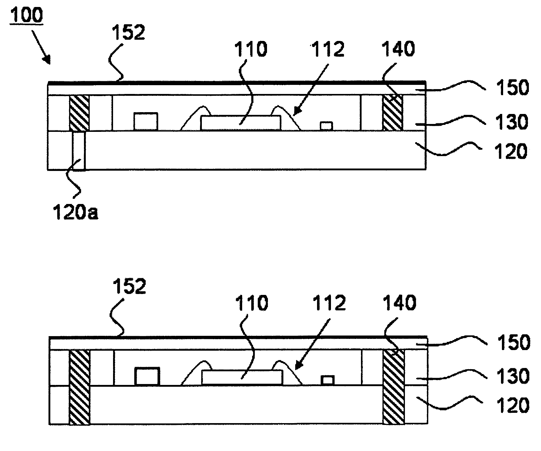
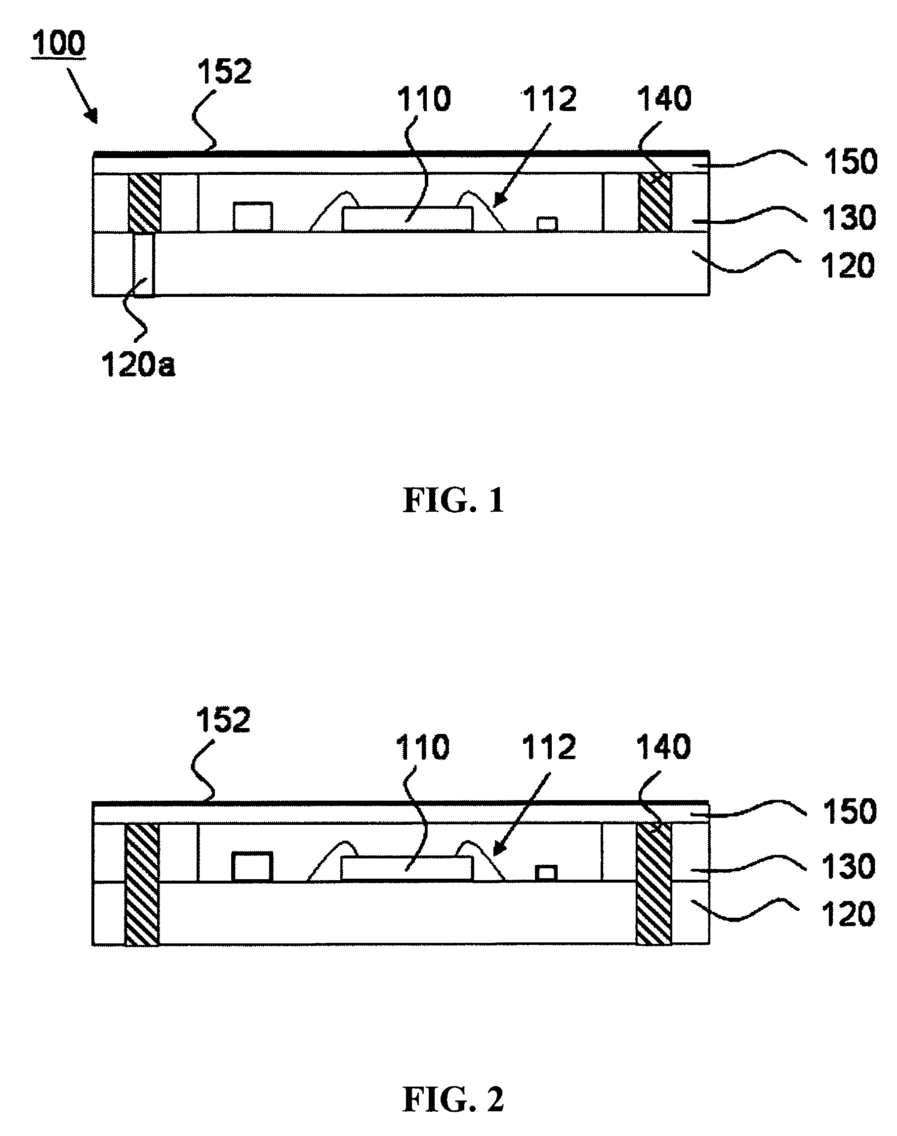
[0023]FIG. 1 illustrates a semiconductor device package 100 according to one embodiment of the present invention. The package 100 includes a semiconductor device 110 attached to a substrate 120 by means of a conductive adhesive (not shown) such as a silver-filled epoxy or a non-conductive adhesive (not shown). As shown, the semiconductor device 110 is connected to the substrate 120 by a plurality of bonding wires 112 which act as electrical input / output (I / O) connections to conductive traces or pads (not shown) of the substrate 120. Alternatively, the semiconductor device 110 may be connected to the substrate 120 by a plurality of solder balls. The solder balls may be formed on an active surface of the semiconductor device 110 using one of any known bumping procedures.

[0024]Referring to FIG. 1, the package 100 is provided with a wall 130 erected from the periphery of the substrate 120 with a height taller than the height of the semiconductor device 110. Note that a metal member 140 ...


PUM


Abstract

A semiconductor device package includes a semiconductor device mounted to a substrate, a wall erected around the semiconductor device with a height taller than the height of the semiconductor device, at least one metal member provided in the wall or against the wall; and a lid secured to the metal member. The metal member and the lid enclose substantially the semiconductor device for providing electromagnetic interference shielding.

Description

BACKGROUND OF THE INVENTION[0001]1. Field of the Invention[0002]This invention relates to semiconductor device packages, and more specifically to semiconductor device packages which are shielded to protect against electromagnetic interference (EMI).[0003]2. Description of the Related Art[0004]Semiconductor device packages typically have electrical circuitry implemented on a circuit substrate, such as a printed circuit board or a ceramic substrate. The performance of the circuitry may be adversely affected by electromagnetic interference (EMI). Electromagnetic interference (EMI) is the generation of undesired electrical signals, or noise, in electronic system circuitry due to the unintentional coupling of impinging electromagnetic field energy.[0005]The coupling of signal energy from an active signal net onto another signal net is referred to as crosstalk. Crosstalk is within-system EMI, as opposed to EMI from a distant source. Crosstalk is proportional to the length of the net paral...

Claims


Application Information

Patent Timeline
Patent Type & Authority Patents(United States)
IPC IPC(8): H01L23/552
CPCH01L23/045H01L23/10H01L23/552H01L2924/07802H01L2224/48227H01L2924/01087H01L2224/48091H01L2924/01079H01L2924/09701H01L2924/16195H01L2924/19105H01L2924/3011H01L2924/3025H01L24/48H01L2924/00014H01L2924/00H01L2224/45099H01L2224/45015H01L2924/207
Inventor YANG, JUNYOUNGKIM, KIDONHAN, JONGHOLEE, JUNHONG
Owner ADVANCED SEMICON ENG INC
Why Eureka
Try Eureka