Chip resistor and manufacturing method therefor

a technology of resistors and manufacturing methods, applied in the direction of resistor chip manufacturing, resistor details, resistors adapted for applying terminals, etc., can solve the problems of increased manufacturing cost, unavoidable certain level of error, and difficult generalization of making such an operational setting accurately, etc., to achieve the effect of convenient manufacturing

Active Publication Date: 2008-02-12
ROHM CO LTD
View PDF13 Cites 32 Cited by
  • Summary
  • Abstract
  • Description
  • Claims
  • Application Information

AI Technical Summary

Benefits of technology

[0007]The present invention was made under the above-described circumstances, and it is therefore an object of the present invention to provide a chip resistor which is easier to manufacture than before, and does not need the resistance value adjustment. Another object of the present invention is to provide a method for manufacturing such a chip resistor.

Problems solved by technology

However, it is not easy in general to make such an operational setting accurately.
Further, in mechanical grinding, it is difficult to achieve an exact dimension for the distance s5 between the two electrodes 91, and therefore a certain level of error is unavoidable.
However, performing the trimming to all of the resistors which are manufactured leads to increased cost of manufacture.

Method used


Image

  • Chip resistor and manufacturing method therefor
  • Chip resistor and manufacturing method therefor
  • Chip resistor and manufacturing method therefor

Examples


first embodiment

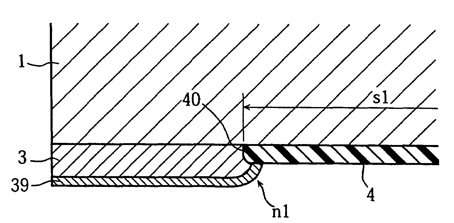
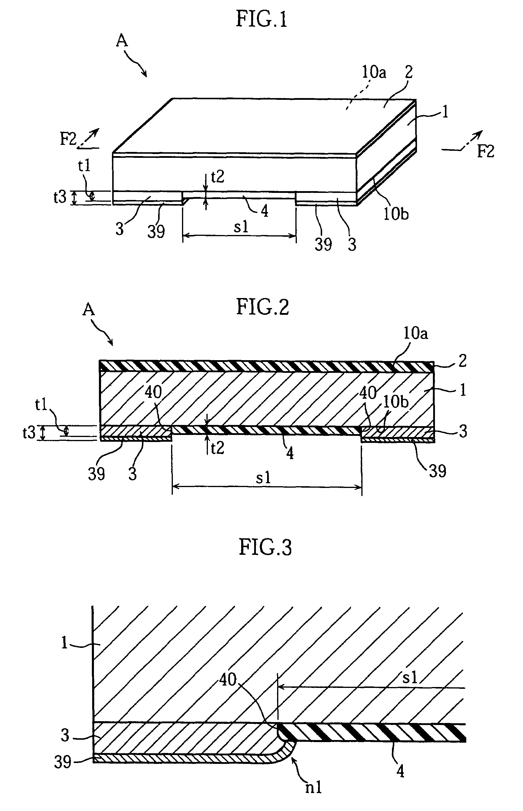
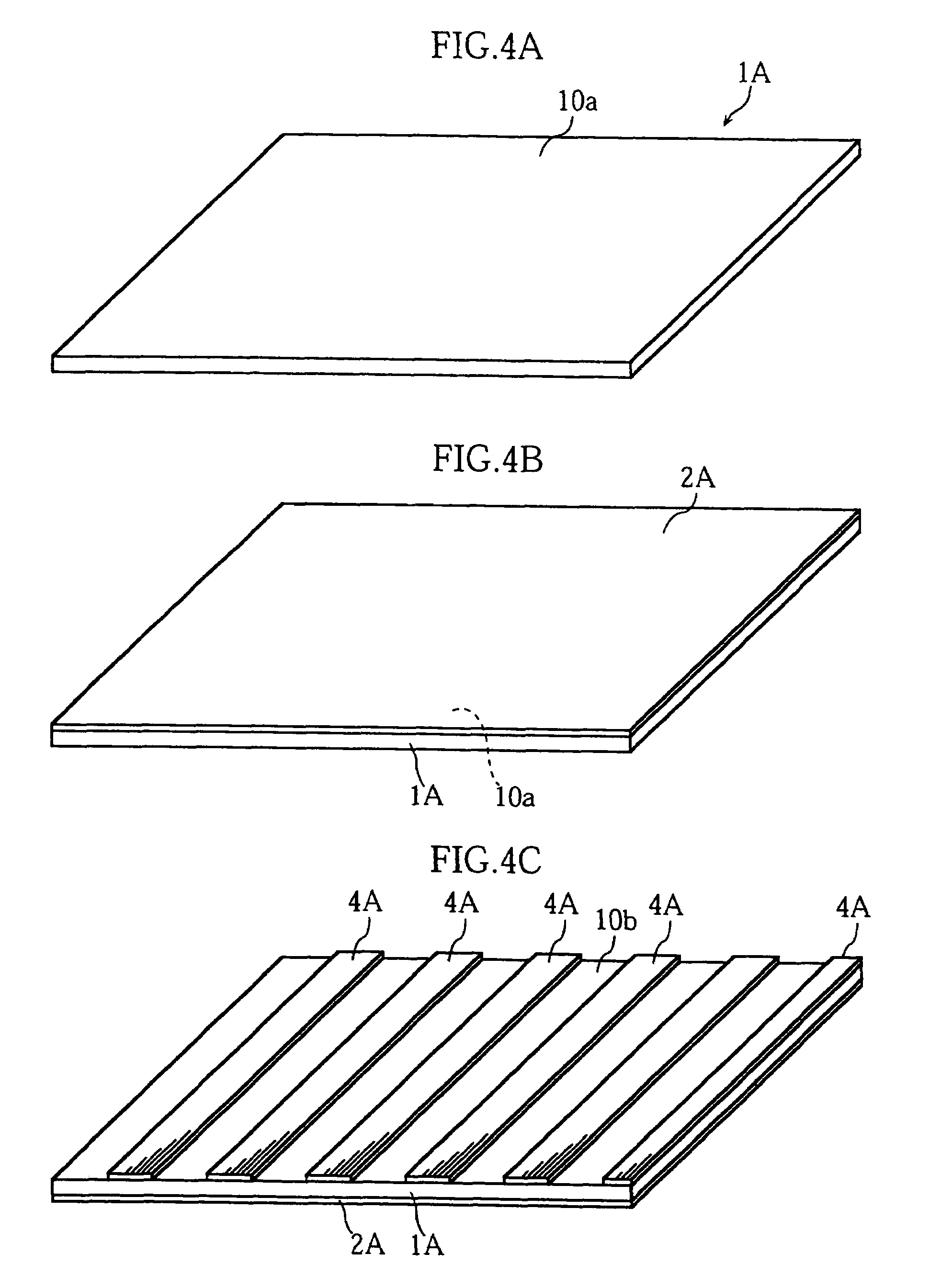
[0048]FIG. 1 through FIG. 3 show a chip resistor A according to the present invention. As shown in FIG. 1 and FIG. 2, the chip resistor A includes a resistive element 1, an overcoat layer 2, a pair of electrodes 3, and an insulating spacer 4.

[0049]The resistive element 1 is a rectangular metal chip. As will be understood from FIG. 2, the resistive element 1 has a uniform thickness. The resistive element 1 is made of e.g. a Cu—Mn alloy, a Ni—Cu alloy and a Ni—Cr alloy. Alternatively, the resistive element 1 can be formed of a nonmetal material.

[0050]The overcoat layer 2 is electrically insulating, and covers an upper surface 10a of the resistive element 1. The overcoat layer 2 can be formed of epoxy resin by thick-film printing.

[0051]The pair of electrodes 3 are on a back surface 10b of the resistive element 1, and are spaced from each other by a predetermined distance s1. The electrodes 3 can be formed by plating copper on the resistive element 1. Each electrode 3 has a lower surfac...

fourth embodiment

[0072]FIG. 12 through FIG. 14 show a chip resistor according to the present invention (the entire resistor is indicated by a reference code Ac). As understood from FIG. 12 and FIG. 13, the chip resistor Ac includes a resistive element 1′, insulation layers 2′ (2a′, 2b′) and a pair of electrodes 3′.

[0073]The resistive element 1′ has a uniform thickness, and is made of a metal material such as a Cu—Mn alloy, a Ni—Cu alloy and a Ni—Cr alloy. Alternatively, the resistive element 1′ may be non-metal. As shown in FIG. 12, the resistive element 1′ is formed with two recesses 11′ which are spaced from each other by a distance s1′.

[0074]The insulation layer 2′ covers an upper surface 10a′ or a back surface 10b′ of the resistive element 1′. The insulation layer 2′ is made of epoxy resin for example.

[0075]The electrode 3′ is formed on a plurality of surfaces 11A′ of the recess 11′ in the resistive element 1′. Therefore, a distance (a minimum distance) between the two electrodes 3′ is equal to ...


PUM

PropertyMeasurementUnit
thickness t3aaaaaaaaaa

Abstract

A chip resistor includes a resistive element (1), an insulation layer (4) formed in a back surface of the flat surface, and two electrodes (3) spaced from each other via the insulation layer. Each electrode (3) makes contact with the insulation layer (4). Each electrode (3) has a lower surface formed with a solder layer (39).

Description

TECHNICAL FIELD[0001]The present invention relates to chip resistors and manufacturing methods therefor.BACKGROUND ART[0002]An example of conventional chip resistors is disclosed in JP-A2002-57009. FIG. 26 of the present application is a sketch of the resistor disclosed in the gazette (The entire resistor is indicated by a reference symbol B). The chip resistor B includes a rectangular resistive element 90 made of metal, and a pair of electrodes 91 formed on a lower surface of the resistive element 90. The two electrodes 91 are spaced from each other by a distance s5. Each electrode 91 has a solder layer 92 formed thereon.[0003]The chip resistor B is manufactured by means of a method shown in FIGS. 27A-27E. First, two metal plates 94, 95 are prepared (FIG. 27A), and the metal plate 95 is bonded to a lower surface of the metal plate 94 (FIG. 27B). The upper metal plate 94 has a relatively larger electric resistance than the lower metal plate 95. The lower metal plate 95 is made of co...

Claims


Application Information

Patent Timeline
Patent Type & Authority Patents(United States)
IPC IPC(8): H01C1/012H01C17/02H01C1/144H01C7/00H01C17/00H01C17/28H05K3/34
CPCH01C1/144H01C7/003H01C17/281H01C17/006Y10T29/49099H05K3/3442H01C7/00H01C17/02
Inventor TSUKADA, TORAYUKI
Owner ROHM CO LTD
Why Eureka
Try Eureka