Three-dimensional semiconductor device provided with interchip interconnection selection means for electrically isolating interconnections other than selected interchip interconnections

a three-dimensional semiconductor and interconnection technology, applied in semiconductor devices, digital storage, instruments, etc., can solve the problems of reducing the capacitance of through-via themselves, the difficulty of accurately forming through-holes in chips with a high aspect ratio, and the limit to miniaturization of semiconductors, so as to achieve high-speed operation and reduce power consumption, the effect of reducing the capacitance of interconnections

Active Publication Date: 2008-02-12
NEC CORP +1
View PDF15 Cites 16 Cited by
  • Summary
  • Abstract
  • Description
  • Claims
  • Application Information

AI Technical Summary

Benefits of technology

[0014]The present invention was realized in view of the above-described problems and has as an object the provision of a three-dimensional semiconductor device that enables both high-speed operation and a reduction in power consumption by reducing the interconnection capacitance of signal interconnections for distributing signals to each of stacked semiconductor circuit chips.
[0016]According to the present invention, when signal transmission is carried out with one particular sub-circuit region among a plurality of sub-circuit regions, only the interchip interconnection to the sub-circuit region that is carrying out signal transmission is selected, and other interchip interconnections are isolated from the selected interchip interconnection. The present invention therefore enables a reduction of the three-dimensional interconnection capacitance of the signal transmission path, and thus enables a reduction of the power consumption of the three-dimensional semiconductor device and higher data transfer speed.

Problems solved by technology

However, because there are limits to miniaturization of semiconductors, new technologies are being sought to achieve further advances in integration density.
This requirement stems from both the difficulty of accurately forming through-holes in a chip with a high aspect ratio due to the restrictions of through-via processing, and the necessity for through-vias that are considerably larger than several μm to achieve the interchip alignment accuracy that is necessary for aligning the positions of through-vias between stacked chips.
In a three-dimensional semiconductor device in which a plurality of chips are stacked and three-dimensional interconnections are implemented, the lowest possible capacitance of the interchip interconnections is demanded, but as described in the foregoing explanation, the through-vias that are used in interchip interconnections have a large profile, and reducing the capacitance of the through-via themselves is problematic.
Reducing the total three-dimensional interconnection capacitance is therefore problematic in the interchip interconnection type, and because interconnection capacitance resulting from in-plane interconnections increases even in the in-plane interconnection type, total three-dimensional interconnection capacitance is extremely difficult to reduce beyond a certain level.

Method used


Image

  • Three-dimensional semiconductor device provided with interchip interconnection selection means for electrically isolating interconnections other than selected interchip interconnections
  • Three-dimensional semiconductor device provided with interchip interconnection selection means for electrically isolating interconnections other than selected interchip interconnections
  • Three-dimensional semiconductor device provided with interchip interconnection selection means for electrically isolating interconnections other than selected interchip interconnections

Examples


first embodiment

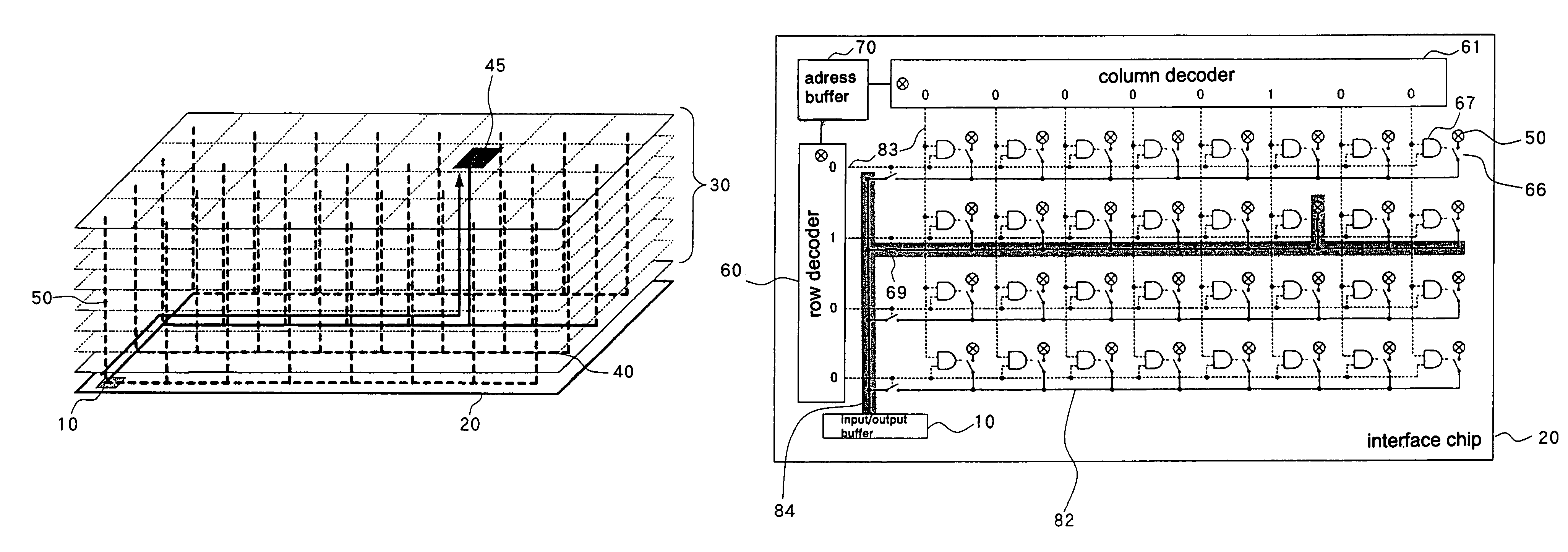
[0045]FIG. 6 shows the configuration of a three-dimensional semiconductor DRAM device, which is a three-dimensional semiconductor device according to the first embodiment of the present invention. In this three-dimensional semiconductor DRAM device, eight memory cell array chips 31 are stacked over interface chip 20 in which circuits for interfacing with the outside are integrated. Memory cell array 63 of 128 Mb, column decoder 61, and row decoder 60 are formed on each memory cell array chip 31.

[0046]Interface chip 20 is provided with a circuit for selecting interchip interconnections, a decoder for controlling this circuit, an address buffer, and input / output buffer 10.

[0047]Memory cell array 63 of each memory cell array chip 31 is composed of a plurality of sub-memory arrays 62 of 4 Mb obtained by dividing memory cell array 63 into eight columns and four rows for a total of 32 sub-memory arrays 62. Each sub-memory array 62 is connected to interface chip 20 by way of a respective i...

second embodiment

[0062]The following explanation regards the second embodiment of a three-dimensional semiconductor device according to the present invention. In the present embodiment, the present invention is applied to a three-dimensional DRAM semiconductor device having a multibank configuration.

[0063]FIG. 9 shows the three-dimensional semiconductor DRAM device that is the second embodiment of the present invention, memory cell array chips 72 each having four banks and the selection of interchip interconnections being carried out when selecting banks. In a multibank configuration, memory cells are accessed by designating addresses in bank units, whereby, when accessing a memory cell of a particular bank, interleaving can be carried out in other banks, this interleaving including precharging operations, or further, operations for selecting word lines and activating bit lines, or refresh operations, and banks can therefore be accessed one after another and data transferred continuously.

[0064]In FI...


PUM


Abstract

In a three-dimensional semiconductor device in which a plurality of semiconductor circuit chips are stacked and that is provided with a plurality of interchip interconnections for signal transmission between these semiconductor circuit chips, when transmitting signals, only one interchip interconnection that serves for signal transmission is selected and other interchip interconnections are electrically isolated by means of switches that are provided between the interchip interconnections and signal lines. Interchip interconnection capacitance relating to the charge and discharge of interconnections is thus minimized.

Description

BACKGROUND OF THE INVENTION[0001]1. Field of the Invention[0002]The present invention relates to a three-dimensional semiconductor device in which a plurality of semiconductor circuit chips are stacked, and more particularly to a three-dimensional semiconductor memory device in which memory cells are formed on stacked semiconductor circuit chips.[0003]2. Description of the Related Art[0004]In recent years, improvements in integration density resulting from the miniaturization of semiconductor integrated circuits have resulted in great advances in the storage capacity in DRAM (Dynamic Random Access Memory) and SRAM (Static Random Access Memory). However, because there are limits to miniaturization of semiconductors, new technologies are being sought to achieve further advances in integration density. Three-dimensional semiconductor devices (stacked semiconductor devices) in which semiconductor circuit chips are stacked have been proposed as one such technology. A method of stacking s...

Claims


Application Information

Patent Timeline
Patent Type & Authority Patents(United States)
IPC IPC(8): G11C5/06G11C7/10G11C8/06G11C8/10G11C8/12G11C7/18H01L25/065H01L27/108
CPCG11C5/02G11C5/063G11C7/18H01L25/0657H01L27/10897H01L2225/06527H01L2225/06541H01L2924/0002H01L2924/00H10B12/50
Inventor SAITO, HIDEAKIHAGIHARA, YASUHIKOFUKAISHI, MUNEOMIZUNO, MASAYUKIIKEDA, HIROAKISHIBATA, KAYOKO
Owner NEC CORP
Why Eureka
Try Eureka