Wide-scan on-chip logic analyzer with global trigger and interleaved SRAM capture buffers

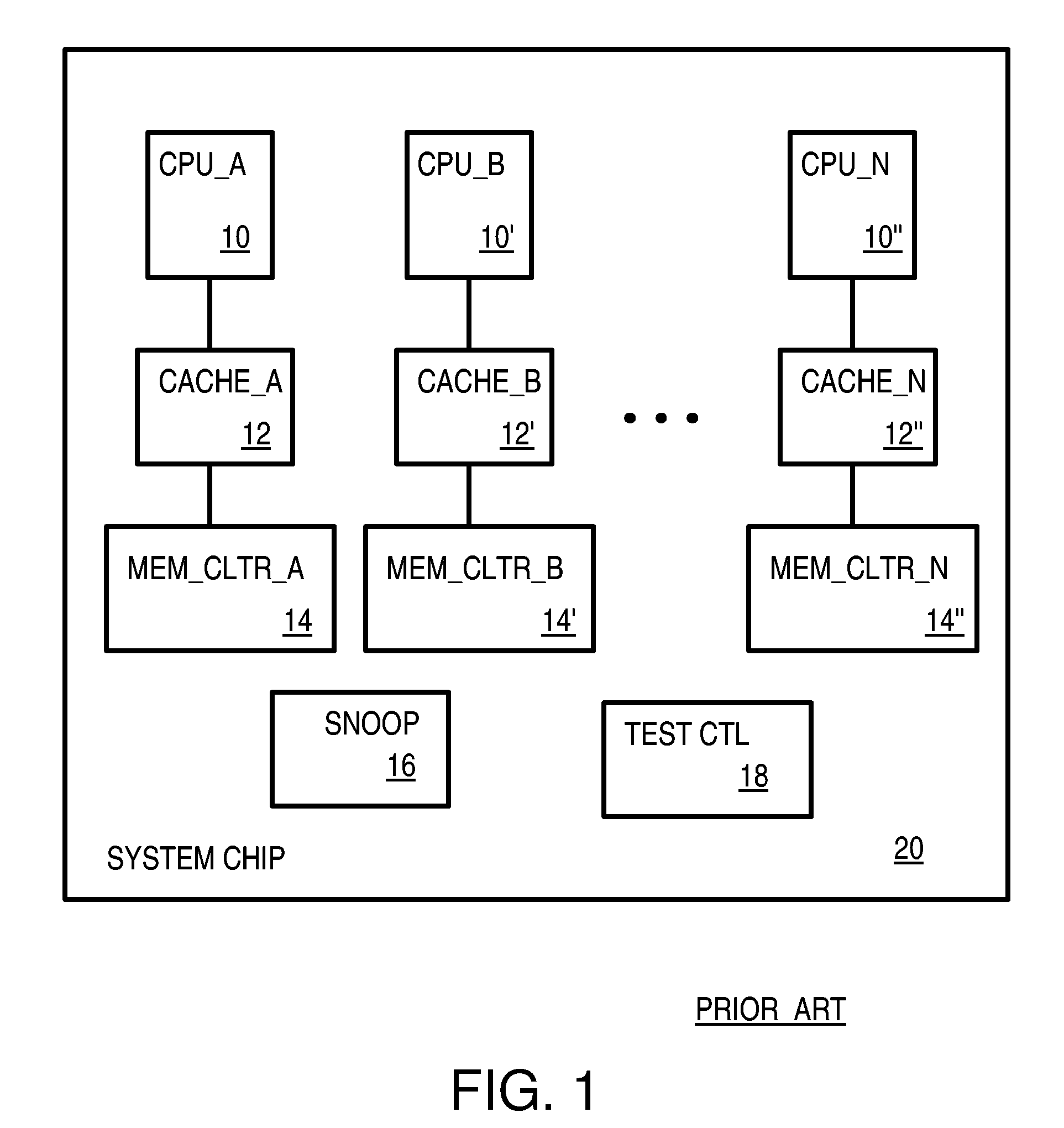
a logic analyzer and logic analysis technology, applied in the direction of error detection/correction, instruments, pulse techniques, etc., can solve the problems of large number of physical wire interfaces to the chip, large number of internal nodes that can be sampled, and difficulty in debugging and testing the chip

Active Publication Date: 2008-02-19
AZUL SYSTEMS
View PDF21 Cites 57 Cited by
  • Summary
  • Abstract
  • Description
  • Claims
  • Application Information

AI Technical Summary

Problems solved by technology

However, the number of physical wire interfaces to the chip are often limited, allowing only a fraction of internal signals to be visible from the chip's I/O.
This makes debug and testing of the chip significantly more difficult, since an external logic analyzer can only observe the chip's I/O.
However, the number of internal nodes that can be sampled is often small.
Sampling may not be possible at full system speeds and may be quite awkward, necessitating time-consuming scan-out of data from serial chains.
A designer cannot know for certain which parts of the chip will have design flaws and will be the subject of an intense debug effort.
However, the additional logic and wiring needed to allow sampling of many internal nodes can be expensive.
However, these buffers can be expensive when many buffers or deep buffers are used.
Control of these buffers can be

Method used


Image

  • Wide-scan on-chip logic analyzer with global trigger and interleaved SRAM capture buffers
  • Wide-scan on-chip logic analyzer with global trigger and interleaved SRAM capture buffers
  • Wide-scan on-chip logic analyzer with global trigger and interleaved SRAM capture buffers

Examples


Embodiment Construction

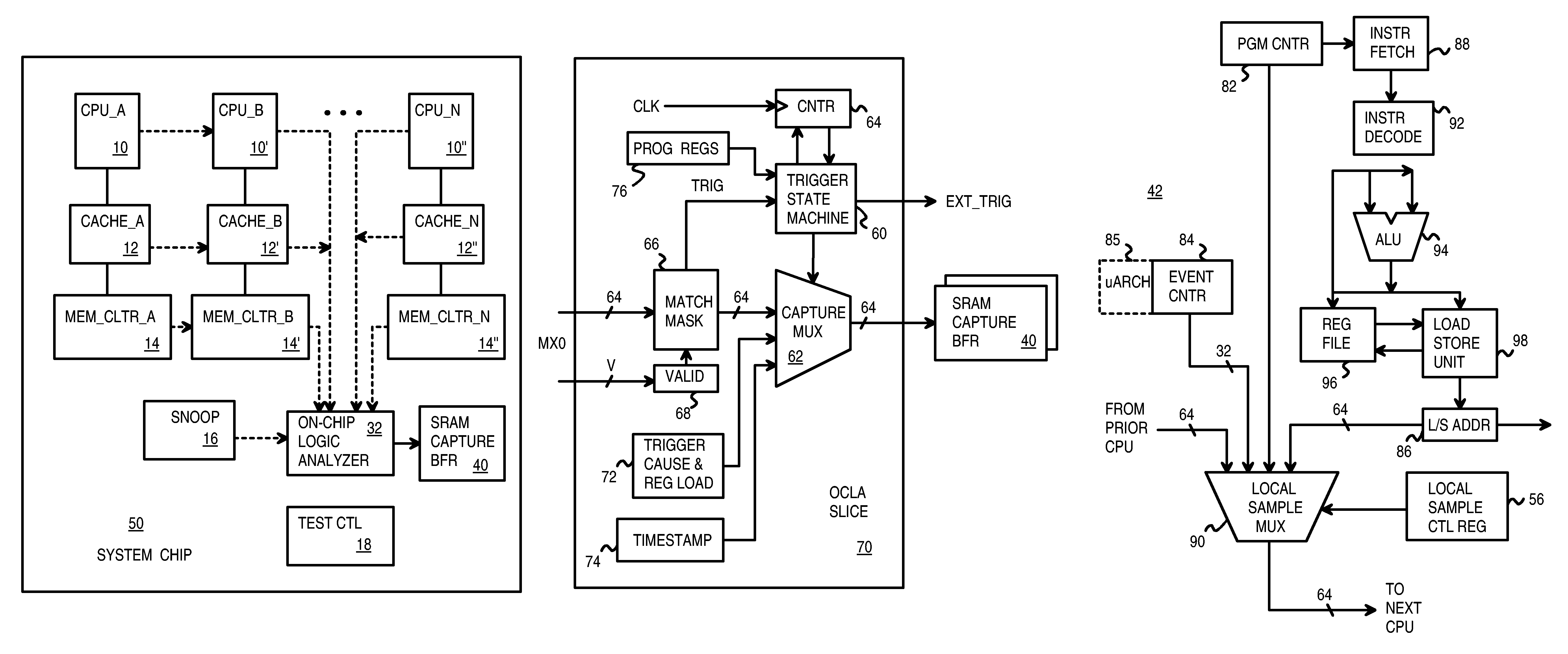
[0026]The present invention relates to an improvement in on-chip logic analyzers. The following description is presented to enable one of ordinary skill in the art to make and use the invention as provided in the context of a particular application and its requirements. Various modifications to the preferred embodiment will be apparent to those with skill in the art, and the general principles defined herein may be applied to other embodiments. Therefore, the present invention is not intended to be limited to the particular embodiments shown and described, but is to be accorded the widest scope consistent with the principles and novel features herein disclosed.

[0027]The inventors have realized that sampling of internal signal nodes on a large chip is inherently distributed across the chip, since the internal nodes are located at different physical locations on the chip. However, storage of the sampled signals can still be centralized, allowing a single debug buffer to store samples ...


PUM


Abstract

A system chip has many local blocks including processor cores, caches, and memory controllers. Each local block has a local sample-select mux that is controlled by a local selection control register. The mux selects from among hundreds of internal sample nodes in the local block, and can also pass through samples output by an upstream local block. The selected samples from local blocks are sent to a central on-chip logic analyzer that compares the samples to a maskable trigger value. When the trigger value is matched, a trigger state machine advances, and samples are stored into a central capture buffer. A user debugging the chip can later read out the central capture buffer at a slower speed. Thousands of internal nodes from local blocks can be selected for sampling, triggering, and debugging. Local blocks include valid bits in 64-bit-wide samples. Only valid samples are written to the capture buffer.

Description

FIELD OF THE INVENTION[0001]This invention relates to integrated circuits, and more particularly to diagnostic circuits for an on-chip logic analyzer.BACKGROUND OF THE INVENTION[0002]Improvements in semiconductor process technology has enabled larger, more complex systems to be integrated onto a single integrated circuit chip. However, the number of physical wire interfaces to the chip are often limited, allowing only a fraction of internal signals to be visible from the chip's I / O. For example, when a large memory and a processor are integrated together as a system-on-a-chip (SOC), the address and data between the processor and the memory may not be visible on the chip's I / O. This makes debug and testing of the chip significantly more difficult, since an external logic analyzer can only observe the chip's I / O.[0003]Internal nodes may be routed to a central block that copies data on the internal nodes to external I / O, such as through using scan chains or JTAG. However, the number of...

Claims


Application Information

Patent Timeline
IPC IPC(8): G06F11/00G01R31/28
CPCG01R31/3177G01R31/318533G11C29/16G11C2029/1208
Inventor NORMOYLE, KEVIN B.REDDY, SREENIVASPHILLIPS, JOHN
Owner AZUL SYSTEMS
Why Eureka
Try Eureka