Charge pump for use in a semiconductor memory

a charge pump and semiconductor technology, applied in the direction of information storage, static storage, digital storage, etc., can solve the problems of degrading the charge transmission efficiency, reducing the efficiency of charge transmission, and difficulty in transferring the charge of boosting node b, so as to achieve efficient charge transmission operation, reduce the threshold voltage increase of the charge transmission transistor, and reduce the body effect

Active Publication Date: 2008-02-19
SAMSUNG ELECTRONICS CO LTD
View PDF5 Cites 6 Cited by
  • Summary
  • Abstract
  • Description
  • Claims
  • Application Information

AI Technical Summary

Benefits of technology

[0015]An exemplary embodiment of the invention provides the charge pump circuit, which is capable of more efficiently reducing the body effect, compared to a conventional method.
[0016]Another exemplary embodiment of the invention provides a charge pump circuit for use in the semiconductor memory device, in which a bulk or substrate of a charge transmission transistor does not float by reducing the body effect. A threshold voltage increase of the charge transmission transistor is substantially reduced to obtain more efficient charge transmission operation. During a charge transfer period a high voltage generation terminal of the charge transmission transistor is connected to the bulk, thus removing the body effect, and during a charge non-transfer period, a latch-up is prevented.

Problems solved by technology

The charge of boosting node B is difficult to sufficiently transfer to the high voltage generation terminal VPP since the gate voltage of the charge transmission transistor N6 is still fixed even though the threshold voltage becomes large.
Thus the charge transmission efficiency can be increased, but the following problems may be caused.
Thus, the increase of threshold voltage may not be prevented or reduced, degrading the charge transmission efficiency.

Method used


Image

  • Charge pump for use in a semiconductor memory
  • Charge pump for use in a semiconductor memory
  • Charge pump for use in a semiconductor memory

Examples


Embodiment Construction

[0024]Exemplary embodiments of the invention are more fully described in detail with reference to FIGS. 4 to 6 in which like components having like functions have been provided with like reference symbols and numerals. The invention may be embodied in many different forms and should not be construed as being limited to the exemplary embodiments set forth herein. Rather, these exemplary embodiments are provided so that this disclosure is thorough and complete, and to convey the concept of the invention to those skilled in the art.

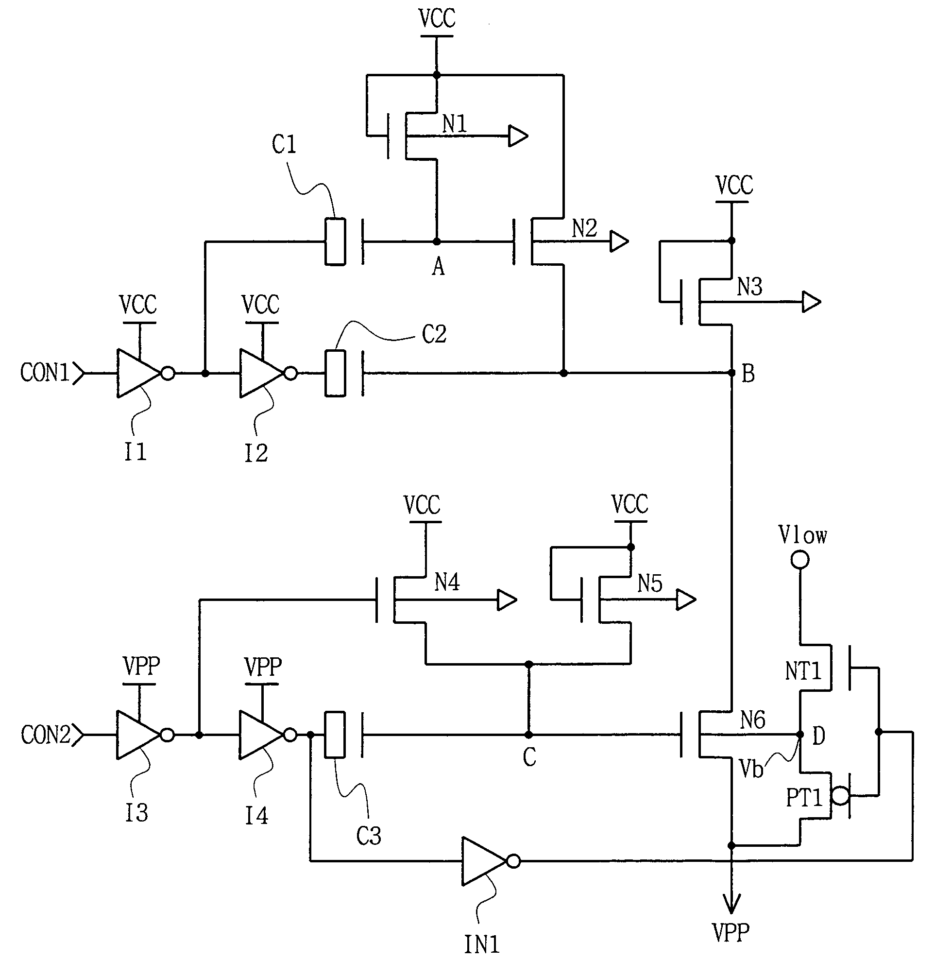
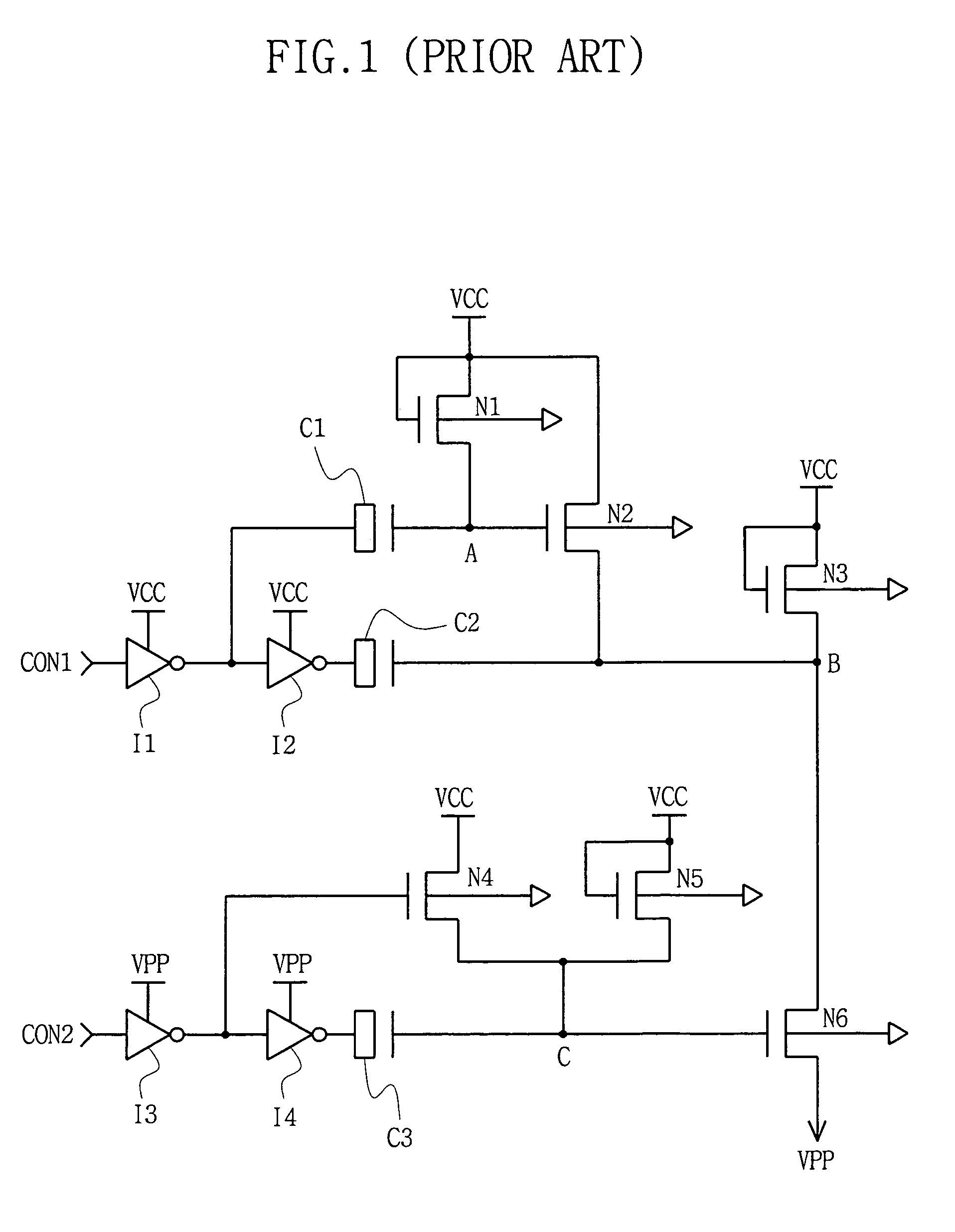
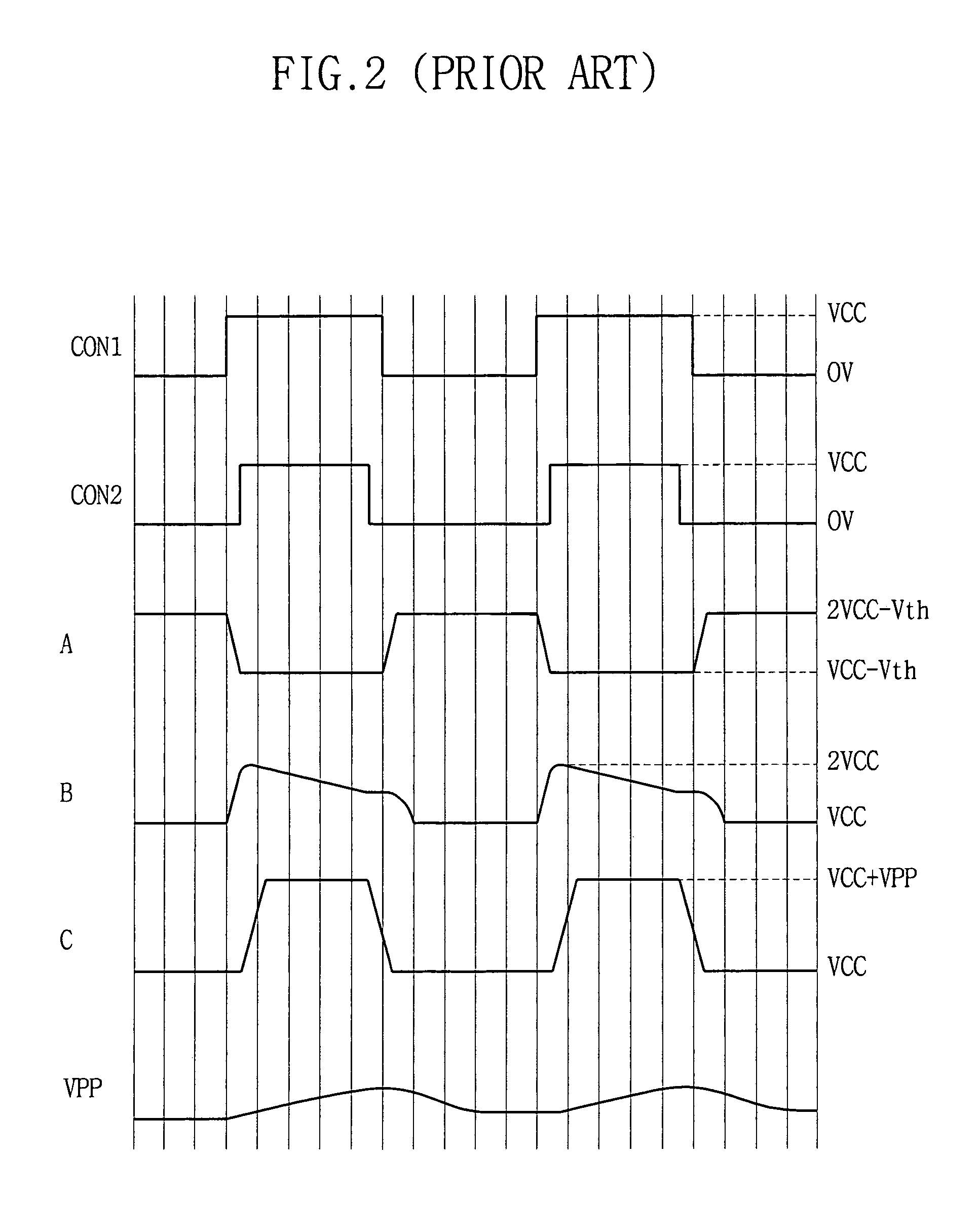
[0025]FIG. 4 is a circuit diagram of a charge pump circuit according to an exemplary embodiment of the invention. Referring to FIG. 4, the charge pump circuit includes a charge pumping portion 50 having a general charge transmission transistor 30 and a bulk connection switch 100. During a charge transfer period a high voltage generation terminal VPP is connected to a bulk Vb of the charge transmission transistor 30, via a PMOS transistor PT1, and during a ch...


PUM


Abstract

In an embodiment, an improved charge pump circuit is provided to control a threshold voltage increase of a charge transmission transistor during a charge transfer period, and to prevent a latch-up generation during a charge non-transfer period. A charge transmission transistor transmits the voltage of a boosting node to a high voltage generation terminal in response to the voltage of a control node. In a bulk connection switch, during the charge transfer period the high voltage generation terminal is connected to the bulk of the charge transmission transistor and during the charge non-transfer period the bulk is connected to the low voltage, being lower than that of the voltage appearing at the boosting node of the charge transmission transistor or the high voltage generation terminal. Charge transmission efficiency and pumping operation reliability are improved, increasing the reliability of data access operations in a semiconductor memory device, for example.

Description

CROSS REFERENCE TO RELATED APPLICATIONS[0001]This application claims priority from Korean Patent Application No. 2004-66380, filed on Aug. 23, 2004, the contents of which are hereby incorporated by reference for all purposes.BACKGROUND OF THE INVENTION[0002]1. Field of the Invention[0003]The present invention relates to a voltage generating circuit for generating a voltage higher than an operating voltage, and more particularly, to a charge pump circuit applied appropriately to a semiconductor memory device.[0004]2. Description of the Related Art[0005]Semiconductor memory devices in recent times tend to have an operating voltage that is lowered to reduce power consumption. But some circuit portions of semiconductor memory, e.g., word line drivers or output drivers, require a high voltage higher than the operating voltage. Thus, charge pump circuits are equipped with most semiconductor memory chips.[0006]Examples of various charge pump circuits are disclosed in U.S. Patent Applicatio...

Claims


Application Information

Patent Timeline
Patent Type & Authority Patents(United States)
IPC IPC(8): G11C7/00
CPCG11C5/145G11C5/14
Inventor YOU, HYUNG-SIKLEE, HYUN-SEOK
Owner SAMSUNG ELECTRONICS CO LTD
Why Eureka
Try Eureka