Power line control circuit of semiconductor device

a technology of power line control and semiconductor devices, which is applied in the direction of semiconductor/solid-state device details, pulse techniques, instruments, etc., can solve the problems of reducing the width of power lines, increasing the manufacturing cost and the manufacturing time of power lines b>11/b> to b>13/b>, and reducing the manufacturing cost and the manufacturing time depending on the formation of power lines

Inactive Publication Date: 2008-02-26
SK HYNIX INC
View PDF5 Cites 7 Cited by
  • Summary
  • Abstract
  • Description
  • Claims
  • Application Information

AI Technical Summary

Benefits of technology

[0013]An embodiment of the present invention is that it provides a power line control circuit of a semiconductor device, in which the width of power lines can be changed easily and the manufacturing cost and the manufacturing time depending on the formation of the power lines can be reduced, by selectively controlling the width of the power lines using dummy power lines.

Problems solved by technology

As a result, the internal voltages transferred through the power lines are lowered due to voltage drop incurred by the resistance of the power lines.
If the internal voltages are lowered as described above, however, the internal circuits may malfunction.
Accordingly, a problem arises because the manufacturing cost and the manufacturing time of the power lines 11 to 13 are increased.

Method used


Image

  • Power line control circuit of semiconductor device
  • Power line control circuit of semiconductor device
  • Power line control circuit of semiconductor device

Examples


first embodiment

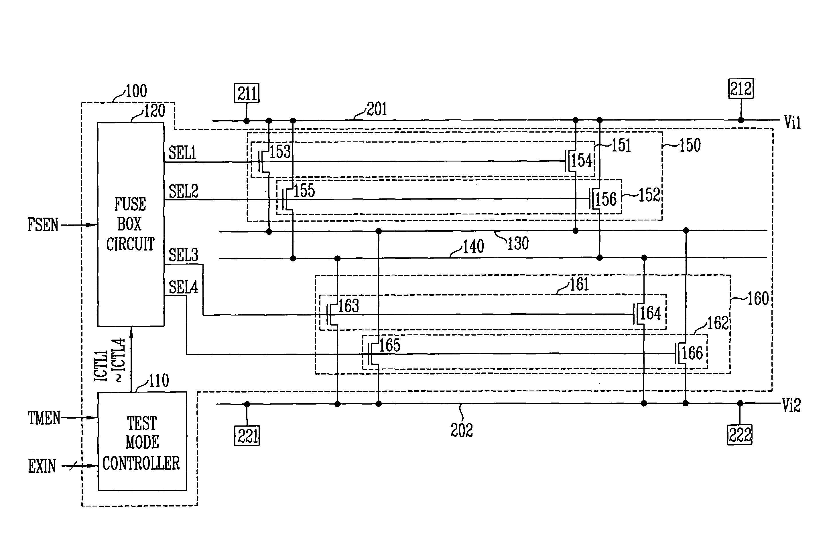
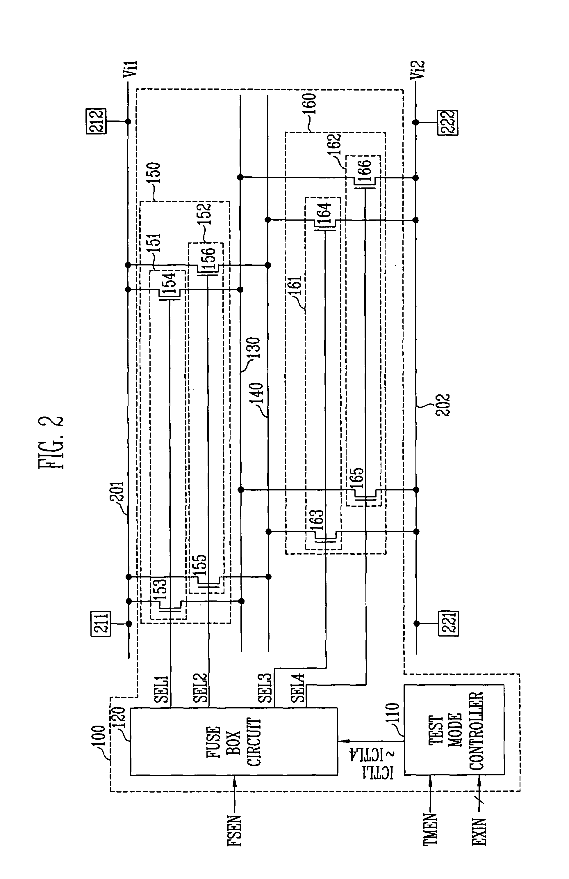
[0028]FIG. 2 is a circuit diagram illustrating a power line control circuit, power lines and internal circuits of a semiconductor device according to the present invention.

[0029]Referring to FIG. 2, the power line control circuit 100 includes a test mode controller 110, a fuse box circuit 120, dummy lines 130, 140, and line width change circuits 150, 160.

[0030]The test mode controller 110 generates control signals ICTL1 to ICTL4 in response to a test mode control signal TMEN and an externally inputted signal EXIN. The externally inputted signal EXIN may be set to N (N is an integer) bits. The test mode controller 110 is enabled or disabled in response to the test mode control signal TMEN.

[0031]For example, when the test mode control signal TMEN is enabled, the test mode controller 110 may be enabled. The test mode controller 110 enables or disables a portion of the control signals ICTL1 to ICTL4 based on a bit value of the externally inputted signal EXIN when being enable. For examp...

second embodiment

[0060]FIG. 4 is a circuit diagram illustrating a power line control circuit, power lines and internal circuits of a semiconductor device according to the present invention.

[0061]Referring to FIG. 4, the power line control circuit 300 includes a test mode controller 310, a fuse box circuit 320, dummy lines DM1, DM2, line width change circuits 330, 340, additional dummy lines FDM1 to FDMJ, SDM1 to SDMJ (J is an integer), and additional line width change circuits 350, 360. The construction and overall operation of the power line control circuit 300 are substantially the same as those of the power line control circuit 100 according to the first embodiment except for several differences. Accordingly, only the differences will be described.

[0062]The power line control circuit 300 is different from the power line control circuit 300 in that it further includes the additional dummy lines FDM1 to FDMJ, SDM1 to SDMJ and the additional line width change circuits 350, 360. The power line contro...

third embodiment

[0074]FIG. 6 is a circuit diagram illustrating a power line control circuit, power lines and internal circuits of a semiconductor device according to the present invention.

[0075]Referring to FIG. 6, the power line control circuit 500 includes a test mode controller 510, a fuse box circuit 520, dummy line groups DG1 to DGM (M is an integer), and line width change circuits FW1 to FWM, SW1 to SWM (M is an integer). The construction and operation of the power line control circuit 500 are substantially the same as those of the power line control circuit 100 according to the first embodiment except for several differences. Accordingly, only the differences will be described.

[0076]The power line control circuit 500 is different from the power line control circuit 100 in that it includes dummy line groups DG1 to DGM and line width change circuits FW1 to FWM, SW1 to SWM. The power line control circuit 500 is also different from the power line control circuit 100 in that the test mode control...


PUM


Abstract

A power line control circuit of a semiconductor device in which a width of a power line can be selectively controlled. The power line control circuit of the semiconductor device according to the present invention can selectively control the width of the power line employing the dummy power line. It is therefore possible to easily change the width of the power lines and to reduce the manufacturing cost and the manufacturing time depending on the formation of the power lines. Furthermore, the power line control circuit of the semiconductor device according to the present invention can selectively control the width of the power lines, if appropriate. Accordingly, mesh of optimized power lines can be provided. Furthermore, more stabilized product characteristics can be secured and the yield of semiconductor memory devices can be enhanced. In addition, the power line control circuit of the semiconductor device according to the present invention can selectively change power mesh corresponding to a power line method or operation mode of a product.

Description

BACKGROUND[0001]1. Field of the Invention[0002]The present invention generally relates to semiconductor devices, and more particularly, to a power line control circuit of a semiconductor device.[0003]2. Discussion of Related Art[0004]In general, internal circuits included in the semiconductor device employ internal voltages, which are generated based on externally supplied and relatively high voltages, as operating power thereof. For this end, the semiconductor device includes power lines for transmitting the internal circuits with the internal voltages, respectively. The arrangement of the power lines and the widths of the power lines may be varied depending on the operating environments of the semiconductor device, the size of the semiconductor device and / or the like.[0005]In recent years, with the developments of semiconductor manufacture technology, the power lines has become minute as the semiconductor device is miniaturized and is more highly integrated. However, as the width ...

Claims


Application Information

Patent Timeline
Patent Type & Authority Patents(United States)
IPC IPC(8): G01R31/02H01L29/00H03K17/00
CPCG01R31/31721G11C5/14G11C29/02G11C29/025G11C29/787
Inventor YANG, JONG YEOL
Owner SK HYNIX INC
Why Eureka
Try Eureka