Method for fabricating ferroelectric capacitive element and ferroelectric capacitive element

a technology of ferroelectric capacitive elements and ferroelectric capacitive elements, which is applied in the direction of capacitors, semiconductor devices, electrical devices, etc., can solve the problems of processing defects of the difficulty of performing necessary refinement processing in forming fine ferroelectric capacitive elements, etc., to achieve the effect of reducing the number of ferroelectric elements, and reducing the number of ferroelectric components

Inactive Publication Date: 2008-03-04
PANASONIC CORP
View PDF4 Cites 5 Cited by
  • Summary
  • Abstract
  • Description
  • Claims
  • Application Information

AI Technical Summary

Benefits of technology

[0018]In consideration of the aforementioned conventional problem, an object of the invention is providing a method for fabricating a ferroelectric capacitive element and a ferroelectric capacitive element in which the composition shift of a ferroelectric capacitor dielectric film is prevented and occurrence of a defect in refinement processing is suppressed without using a platinum film.
[0063]Alternatively, in the ferroelectric capacitive element of this invention, since the bismuth concentration in the ferroelectric film obtained after annealing is substantially homogeneous, the composition shift is prevented, so that the ferroelectric film can attain a sufficient ferroelectric characteristic. Also, without using a platinum film as in the conventional technique for preventing the composition shift of the ferroelectric film, the metal film more easily dry etched than a platinum film is used, and therefore, the occurrence of a processing defect of the ferroelectric capacitive element, which derives from generation of particles or the like occurring during dry etching, can be prevented. Moreover, since the layer including the group V element and bismuth is formed between the ferroelectric film and the lower electrode or between the ferroelectric film and the upper electrode, the bismuth diffused from the ferroelectric film can be efficiently captured by the layer including the group V element and the bismuth. Therefore, when the layer having captured the bismuth is analyzed, the amount of bismuth diffused from and going out of the ferroelectric film can be previously grasped, and hence, the composition of the ferroelectric film can be more effectively controlled. As a result, the ferroelectric capacitive element can attain a good ferroelectric characteristic.

Problems solved by technology

The present inventors have found that in various structures of a conventional ferroelectric capacitive element, since a platinum thin film is disposed between a ferroelectric capacitor dielectric film and a conductive ceramic film, it is very difficult to perform necessary refinement processing in forming a fine ferroelectric capacitive element.
Accordingly, in realizing the conventional structure of the ferroelectric capacitive element by the refinement processing, although the diffusion of the composition of the ferroelectric capacitor dielectric film can be prevented by the platinum thin films disposed on and below the ferroelectric capacitor dielectric film, the particles cause processing defects of the fine ferroelectric capacitive element.

Method used


Image

  • Method for fabricating ferroelectric capacitive element and ferroelectric capacitive element
  • Method for fabricating ferroelectric capacitive element and ferroelectric capacitive element
  • Method for fabricating ferroelectric capacitive element and ferroelectric capacitive element

Examples


embodiment 1

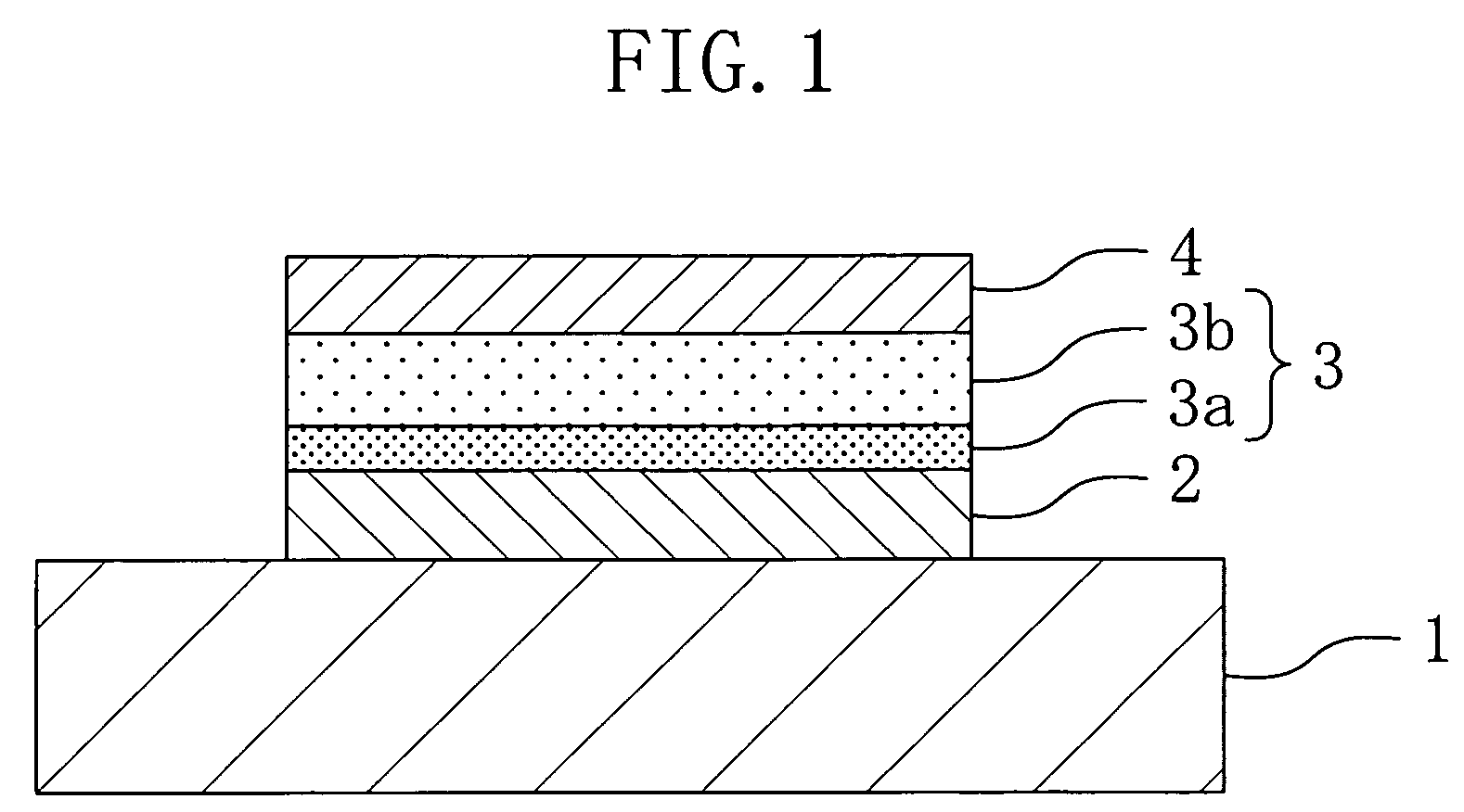
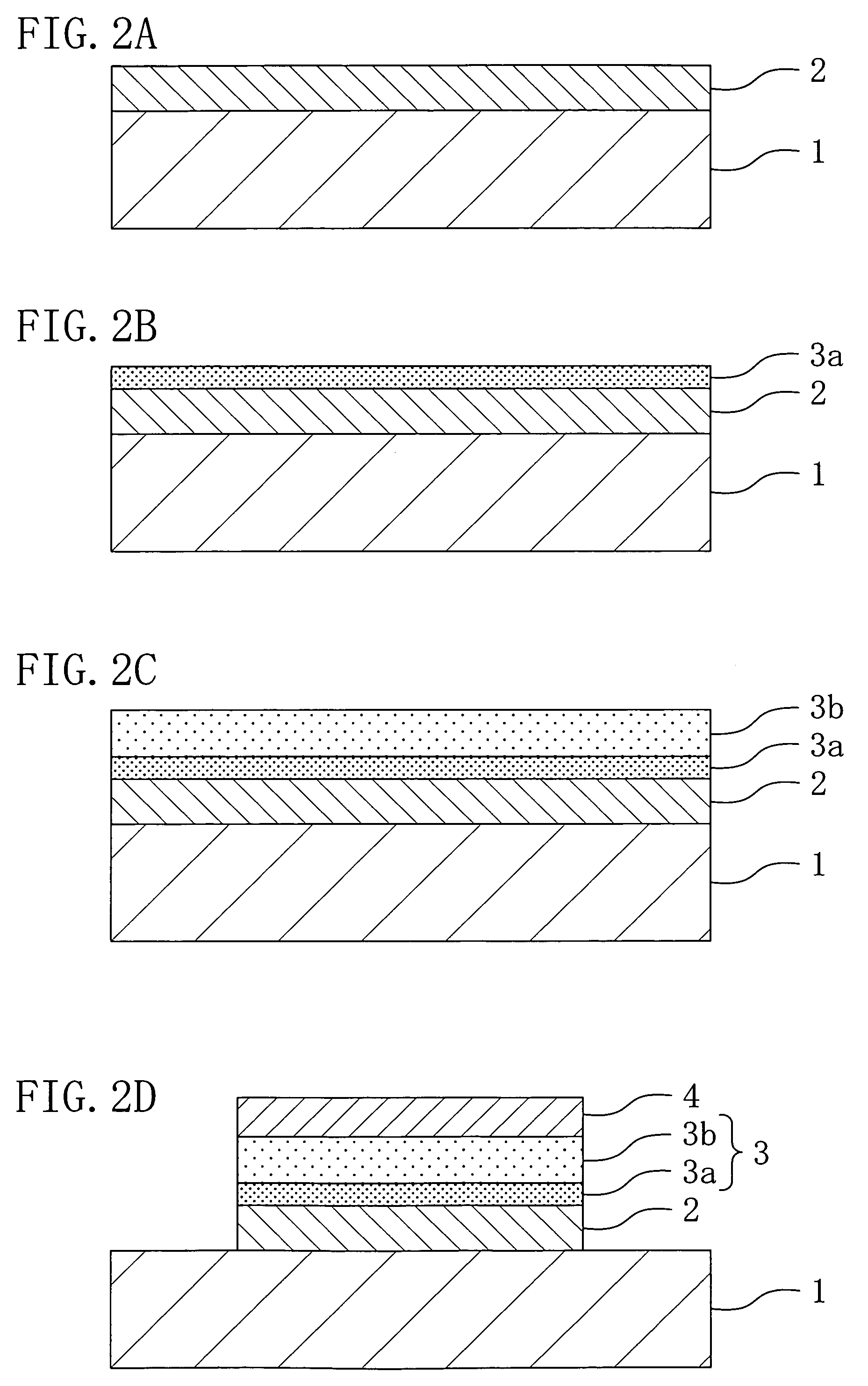
[0080]Now, a semiconductor device including a ferroelectric capacitive element according to Embodiment 1 of the invention will be described with reference to FIG. 1.

[0081]FIG. 1 is a cross-sectional view for showing the structure of a principal part of the semiconductor device including the ferroelectric capacitive element of Embodiment 1.

[0082]As shown in FIG. 1, a MOS transistor (not shown) for providing a function as a semiconductor memory device to the semiconductor device is formed on a substrate 1 made of a semiconductor substrate of monosilicon or the like or an insulating substrate of quartz or the like. It is noted that a semiconductor thin film such as a polysilicon film, an amorphous silicon film, a SiO2 film or a silicon nitride film, an aluminum interconnect layer or a Cu interconnect layer may be formed on the substrate 1.

[0083]A lower electrode 2 made of a metal film more easily etched than a platinum film, such as a noble metal oxide film or a multilayered film of a ...

embodiment 2

[0108]A semiconductor device including a ferroelectric capacitive element according to Embodiment 2 of the invention will now be described with reference to FIG. 6.

[0109]FIG. 6 is a cross-sectional view for showing the structure of a principal part of the semiconductor device including the ferroelectric capacitive element of Embodiment 2.

[0110]As shown in FIG. 6, a MOS transistor (not shown) for providing a function as a semiconductor memory device to the semiconductor device is formed on a substrate 10 made of a semiconductor substrate of monosilicon or the like or an insulating substrate of quartz or the like. It is noted that a semiconductor thin film such as a polysilicon film, an amorphous silicon film, a SiO2 film or a silicon nitride film, an aluminum interconnect layer or a Cu interconnect layer may be formed on the substrate 10.

[0111]On the substrate 10, a lower electrode 11 made of a metal film more easily dry etched than a platinum film, such as a noble metal oxide film o...

embodiment 3

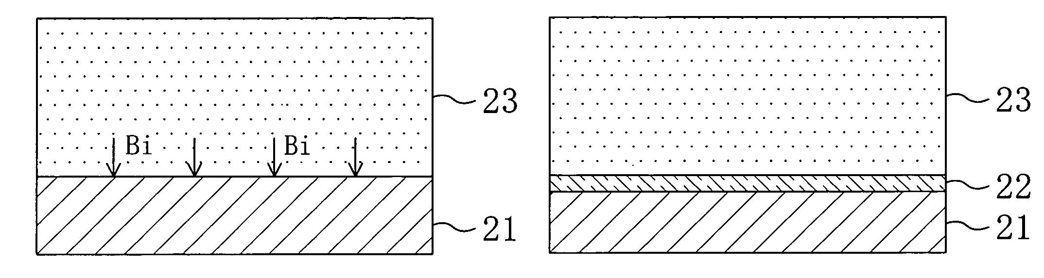
[0124]A semiconductor device including a ferroelectric capacitive element according to Embodiment 3 of the invention will now be described with reference to FIG. 9.

[0125]FIG. 9 is a cross-sectional view for showing the structure of a principal part of the ferroelectric capacitive element of Embodiment 3.

[0126]As shown in FIG. 9, a lower electrode 21 is formed on a substrate (not shown) made of a semiconductor substrate of monosilicon or the like or an insulating substrate of quartz or the like. A material used for forming the lower electrode 21 includes a group V element, and the lower electrode 21 is made from, for example, IrTa, IrPa, IrNb, IrTaOx, IrPaOx or IrNbOx. Also, the lower electrode 21 preferably has a thickness of 100 through 500 nm, and the material including the group V element may be used merely in an upper portion with a thickness of 50 through 100 nm of the lower electrode 21. It is noted that a MOS transistor for providing a function as a semiconductor memory devic...


PUM

PropertyMeasurementUnit
sizeaaaaaaaaaa
thicknessaaaaaaaaaa
thicknessaaaaaaaaaa

Abstract

A method for fabricating a ferroelectric capacitive element of this invention includes the steps of forming a lower electrode made of a first conductive film on a substrate; forming a first ferroelectric film including bismuth in a first concentration on the lower electrode; forming a second ferroelectric film including bismuth in a second concentration on the first ferroelectric film; performing annealing after forming the first ferroelectric film and the second ferroelectric film; and forming an upper electrode made of a second conductive film on the second ferroelectric film after the annealing. The first conductive film is a metal film more easily etched than a platinum film, and the second ferroelectric film is formed in such a manner that the second concentration is lower than the first concentration before the annealing.

Description

CROSS-REFERENCE TO RELATED APPLICATIONS[0001]This application claims priority under 35 U.S.C. § 119 on Patent Application Nos. 2004-89545 and 2004-357172 filed in Japan respectively on Mar. 25, 2004 and Dec. 9, 2004, the entire contents of which are hereby incorporated by reference.BACKGROUND OF THE INVENTION[0002]The present invention relates to a ferroelectric capacitive element using, as a capacitor dielectric film, a bismuth-based layered perovskite type ferroelectric, that is, a dielectric metal oxide, thin film (hereinafter simply referred to as the ferroelectric thin film), and more particularly, it relates to a structure of the ferroelectric thin film and a method for forming the ferroelectric thin film.[0003]Recently, there is a trend toward using an oxide film of a bismuth-based, and specifically, an SBT-based or a BST-based layered perovskite type as a ferroelectric thin film working as a capacitor dielectric film. Such an oxide film is applied to a semiconductor electron...

Claims


Application Information

Patent Timeline
Patent Type & Authority Patents(United States)
IPC IPC(8): H01L21/00H01L27/04H01L21/02H01L21/316H01L21/822H01L21/8246H01L27/105H01L29/76H01L29/78H01L29/94
CPCH01L29/78391H01L28/56
Inventor TATSUNARI, TOSHITAKA
Owner PANASONIC CORP
Why Eureka
Try Eureka