Method for fabricating ferroelectric capacitive element and ferroelectric capacitive element
a technology of ferroelectric capacitive elements and ferroelectric capacitive elements, which is applied in the direction of capacitors, semiconductor devices, electrical devices, etc., can solve the problems of processing defects of the difficulty of performing necessary refinement processing in forming fine ferroelectric capacitive elements, etc., to achieve the effect of reducing the number of ferroelectric elements, and reducing the number of ferroelectric components
- Summary
- Abstract
- Description
- Claims
- Application Information
AI Technical Summary
Benefits of technology
Problems solved by technology
Method used
Image
Examples
embodiment 1
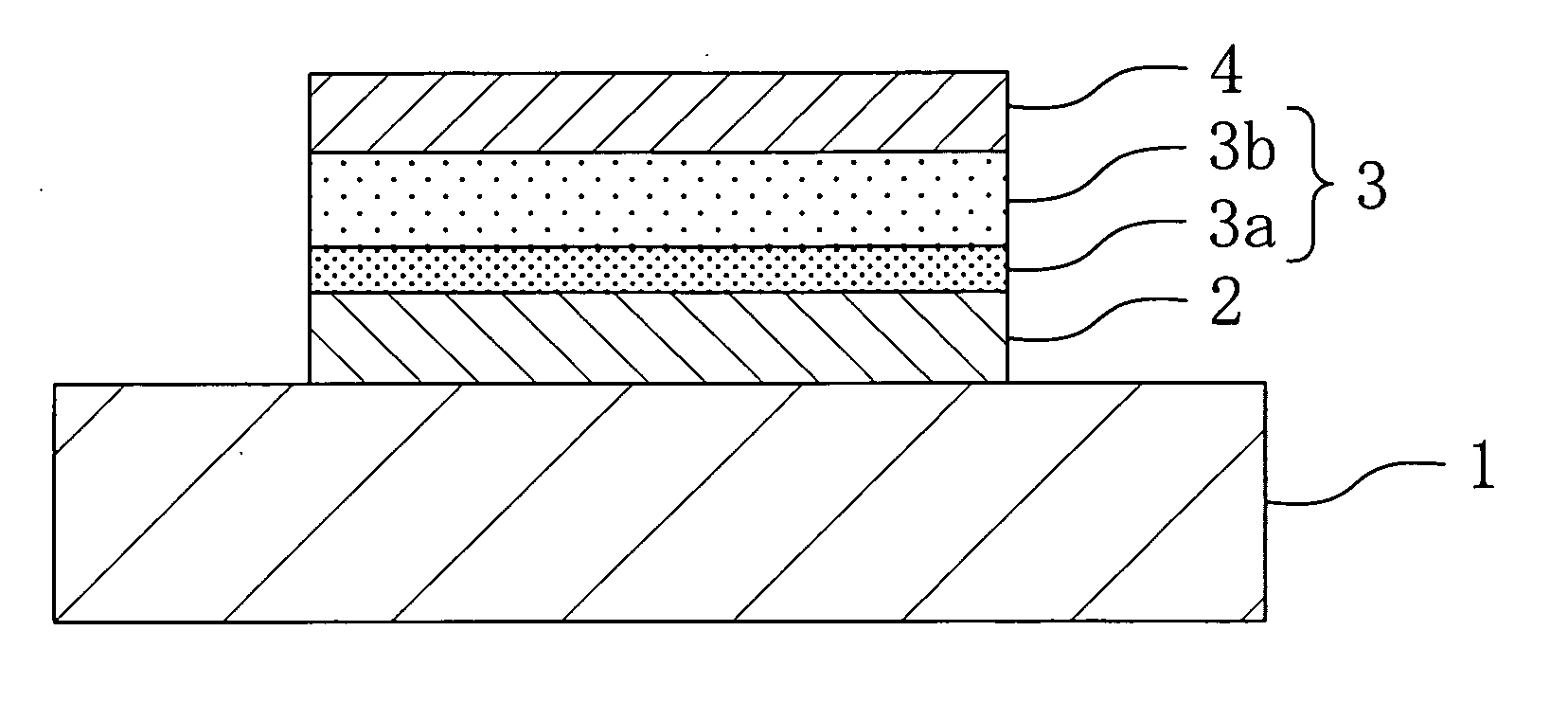
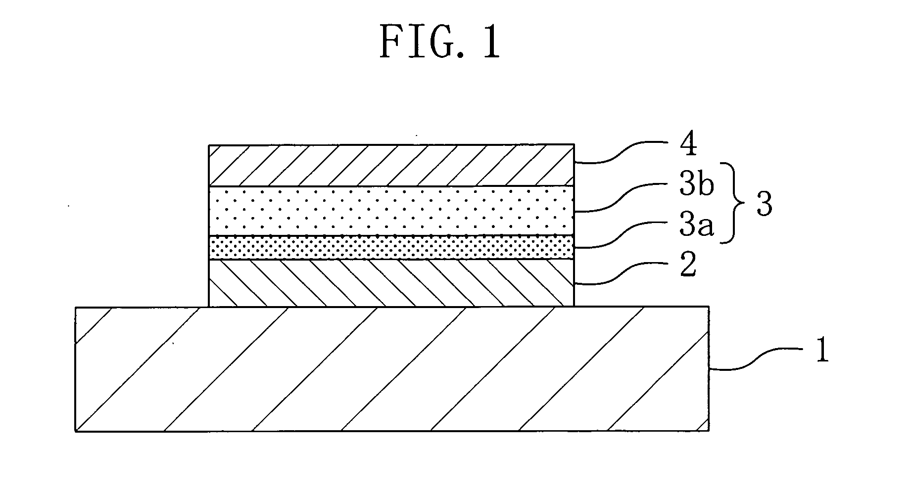
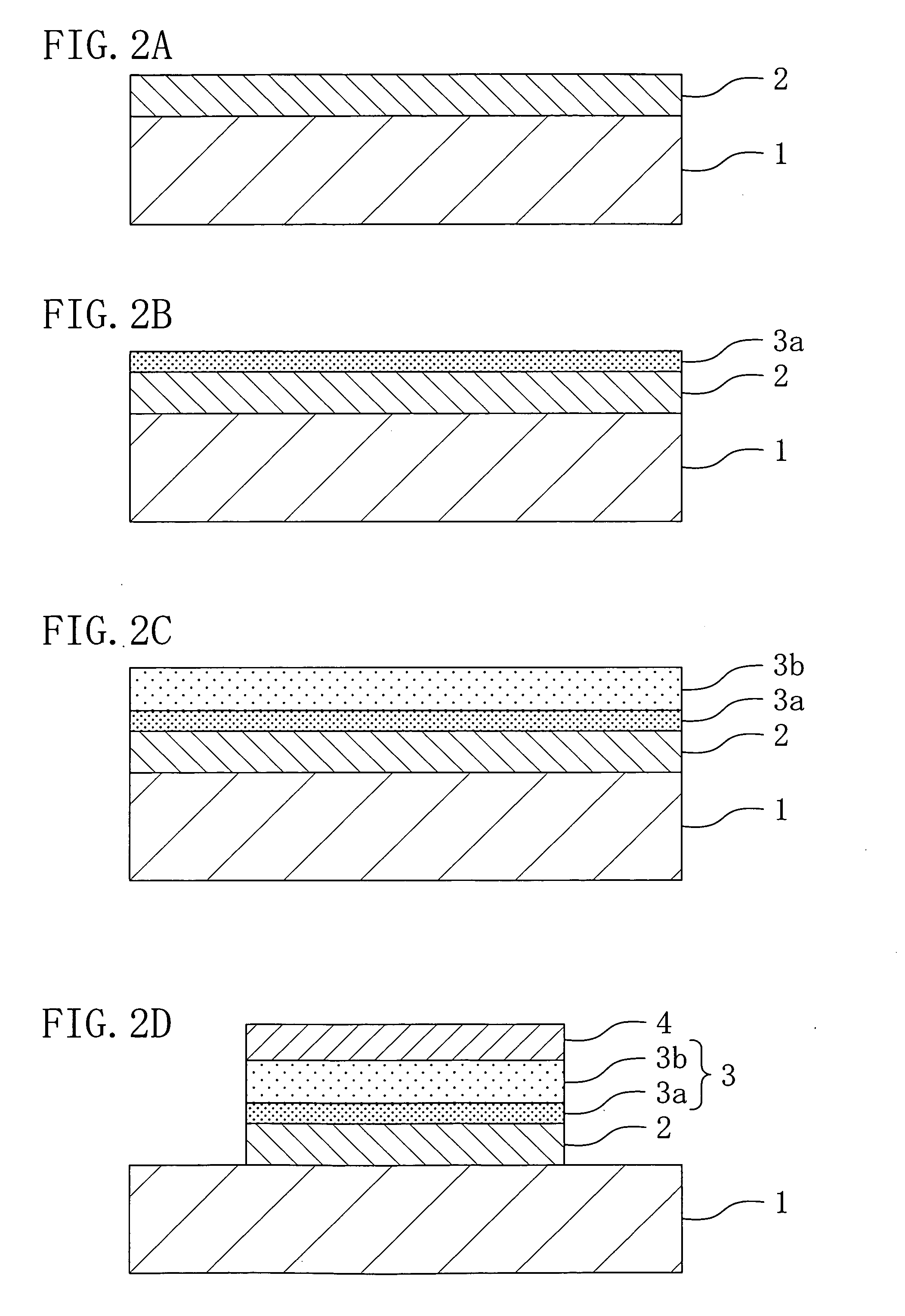
[0080] Now, a semiconductor device including a ferroelectric capacitive element according to Embodiment 1 of the invention will be described with reference to FIG. 1.
[0081]FIG. 1 is a cross-sectional view for showing the structure of a principal part of the semiconductor device including the ferroelectric capacitive element of Embodiment 1.
[0082] As shown in FIG. 1, a MOS transistor (not shown) for providing a function as a semiconductor memory device to the semiconductor device is formed on a substrate 1 made of a semiconductor substrate of monosilicon or the like or an insulating substrate of quartz or the like. It is noted that a semiconductor thin film such as a polysilicon film, an amorphous silicon film, a SiO2 film or a silicon nitride film, an aluminum interconnect layer or a Cu interconnect layer may be formed on the substrate 1.
[0083] A lower electrode 2 made of a metal film more easily etched than a platinum film, such as a noble metal oxide film or a multilayered film...
embodiment 2
[0108] A semiconductor device including a ferroelectric capacitive element according to Embodiment 2 of the invention will now be described with reference to FIG. 6.
[0109]FIG. 6 is a cross-sectional view for showing the structure of a principal part of the semiconductor device including the ferroelectric capacitive element of Embodiment 2.
[0110] As shown in FIG. 6, a MOS transistor (not shown) for providing a function as a semiconductor memory device to the semiconductor device is formed on a substrate 10 made of a semiconductor substrate of monosilicon or the like or an insulating substrate of quartz or the like. It is noted that a semiconductor thin film such as a polysilicon film, an amorphous silicon film, a SiO2 film or a silicon nitride film, an aluminum interconnect layer or a Cu interconnect layer may be formed on the substrate 10.
[0111] On the substrate 10, a lower electrode 11 made of a metal film more easily dry etched than a platinum film, such as a noble metal oxide ...
embodiment 3
[0124] A semiconductor device including a ferroelectric capacitive element according to Embodiment 3 of the invention will now be described with reference to FIG. 9.
[0125]FIG. 9 is a cross-sectional view for showing the structure of a principal part of the ferroelectric capacitive element of Embodiment 3.
[0126] As shown in FIG. 9, a lower electrode 21 is formed on a substrate (not shown) made of a semiconductor substrate of monosilicon or the like or an insulating substrate of quartz or the like. A material used for forming the lower electrode 21 includes a group V element, and the lower electrode 21 is made from, for example, IrTa, IrPa, IrNb, IrTaOx, IrPaOx or IrNbOx. Also, the lower electrode 21 preferably has a thickness of 100 through 500 nm, and the material including the group V element may be used merely in an upper portion with a thickness of 50 through 100 nm of the lower electrode 21. It is noted that a MOS transistor for providing a function as a semiconductor memory d...
PUM
 Abstract
Description
Claims
Application Information


