Surface mount crystal oscillator

a crystal oscillator and surface mount technology, applied in the field of crystal oscillators, can solve the problems of high oscillation frequency of oscillators, achieve good oscillation characteristics, facilitate a reduction in size, and suppress the occurrence of stress

Inactive Publication Date: 2008-03-04
NIHON DEMPA KOGYO CO LTD
View PDF6 Cites 9 Cited by
  • Summary
  • Abstract
  • Description
  • Claims
  • Application Information

AI Technical Summary

Benefits of technology

[0021]It is an object of the present invention to provide a surface mount crystal oscillator which has an IC chip and a crystal blank integrated therein, suppresses the occurrence of a stress on the crystal blank to maintain good oscillation characteristics, and facilitates a reduction in size.
[0023]In the configuration as described above, the crystal blank can be excited by the first excitation electrode disposed on the first principal surface of the crystal blank and the second excitation electrode disposed on the IC chip, using the space field method on the second principal surface of the crystal blank. Then, since the IC chip is bonded to the crystal blank directly, the resulting surface-mount crystal oscillator is reduced in size. Also, the crystal blank is secured to the IC chip only at one point in its peripheral region, thus suppressing a distortion in the crystal blank caused by a difference in coefficient of thermal expansion between the IC chip and the crystal blank, as compared with a crystal blank secured at two points in a periphery region.
[0024]In the present invention, a depressed portion may be formed in the first principal surface of the crystal blank, such that the crystal blank is reduced in thickness in the area of this depressed portion, and this area serves as a vibration region. A first excitation electrode may be formed on the bottom of the depressed portion, and an extension electrode may extend to a relatively thick region around the depressed portion to be secured to the first crystal connection terminal. Such a configuration results in a surface mount crystal oscillator which provides high oscillation frequencies. In this event, a first crystal plate having a through-hole is directly bonded to a second crystal plate having a flat shape to constitute a crystal blank, thereby making the thickness uniform in the vibration region of the crystal blank to exhibit better oscillation characteristics. Further, a cavity having a depth smaller than the depressed portion is formed in the second principal surface of the crystal blank corresponding to the position of the depressed portion, thereby ensuring that a gap is maintained between the vibration region of the crystal blank and the first principal surface of the IC chip to eliminate impediments to oscillation due to the first principal surface of the IC chip coming in contact with the vibration region.

Problems solved by technology

Such a configuration results in a surface mount crystal oscillator which provides high oscillation frequencies.

Method used


Image

  • Surface mount crystal oscillator
  • Surface mount crystal oscillator
  • Surface mount crystal oscillator

Examples


first embodiment

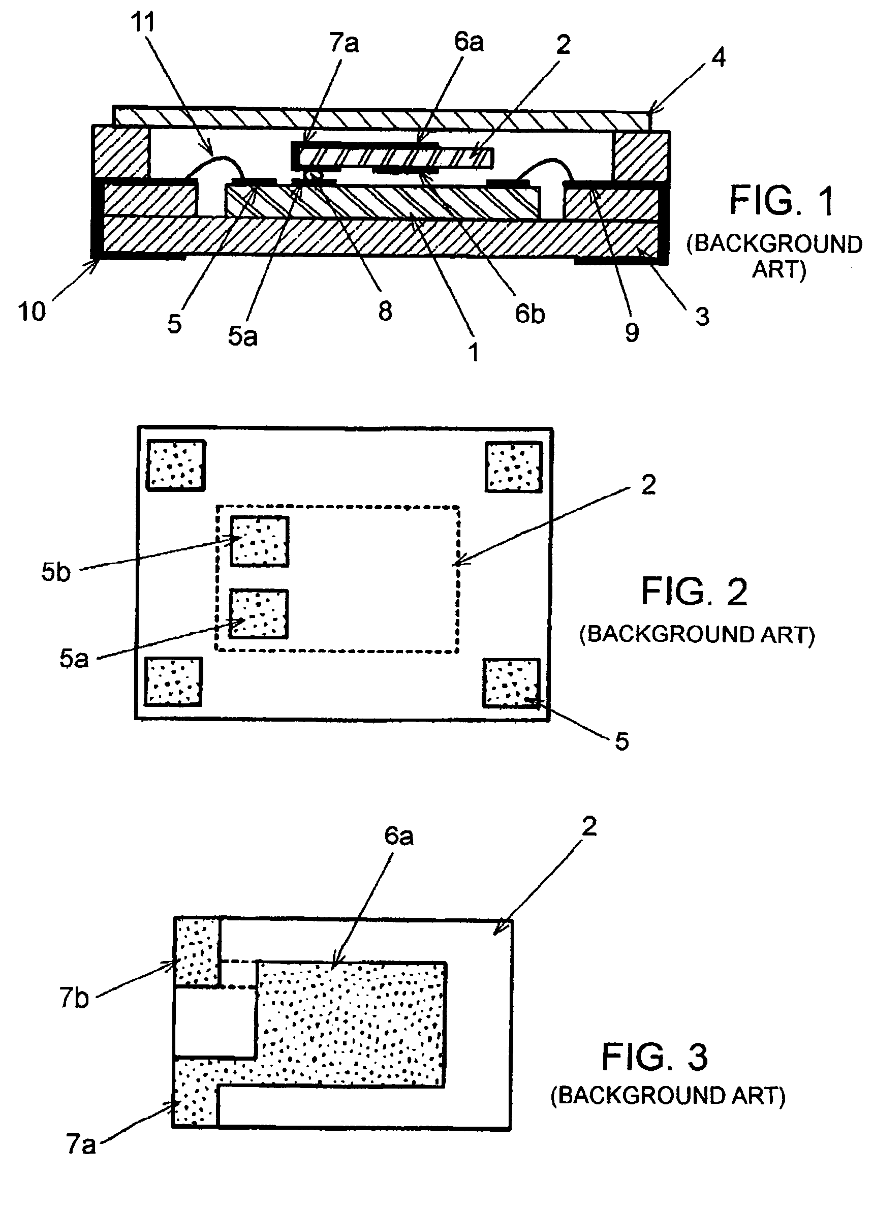
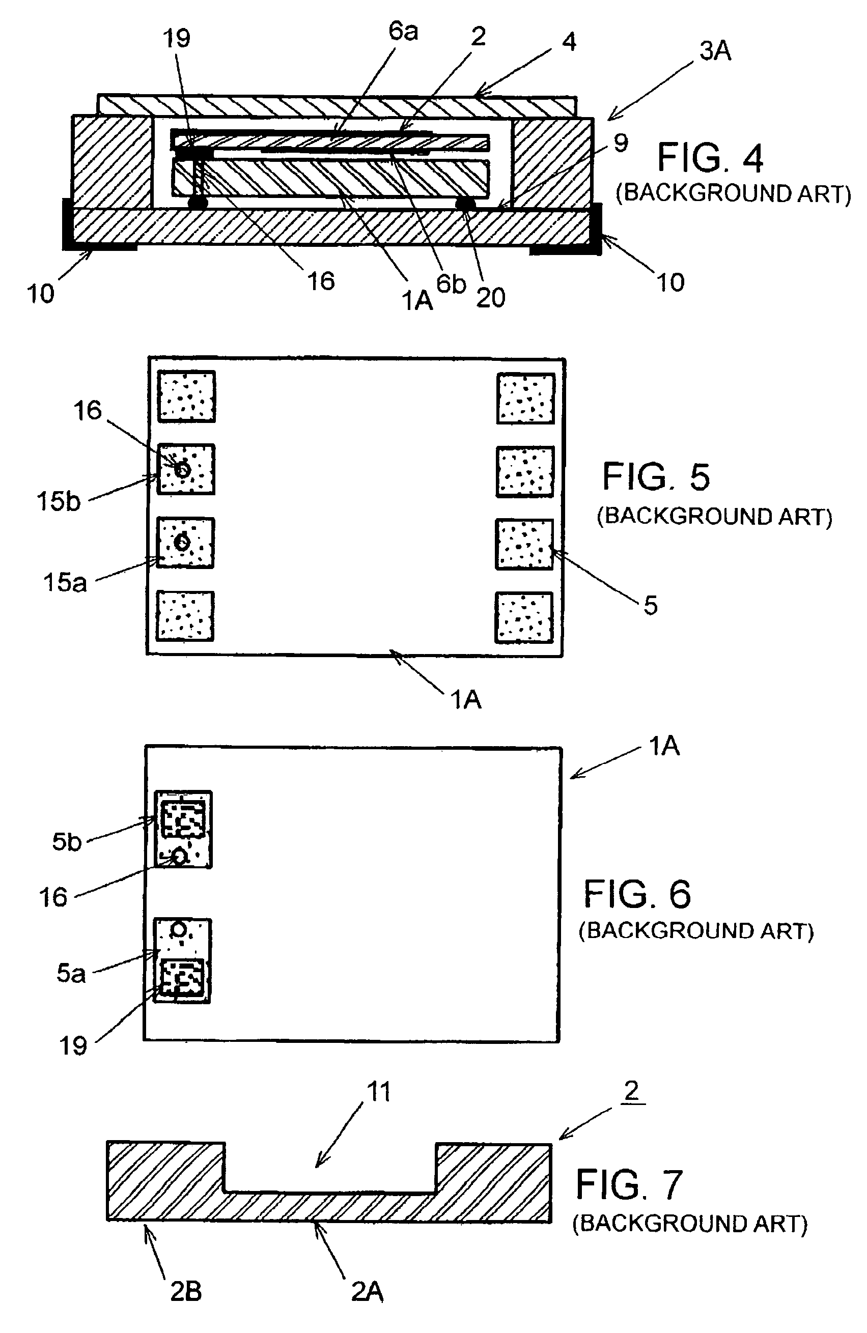
[0042]FIG. 8 illustrates a surface mount crystal oscillator according to the present invention. In the following description, components identical to those inFIGS. 1 to 7 are designated the same reference numerals, and repetitive descriptions thereon will be simplified.

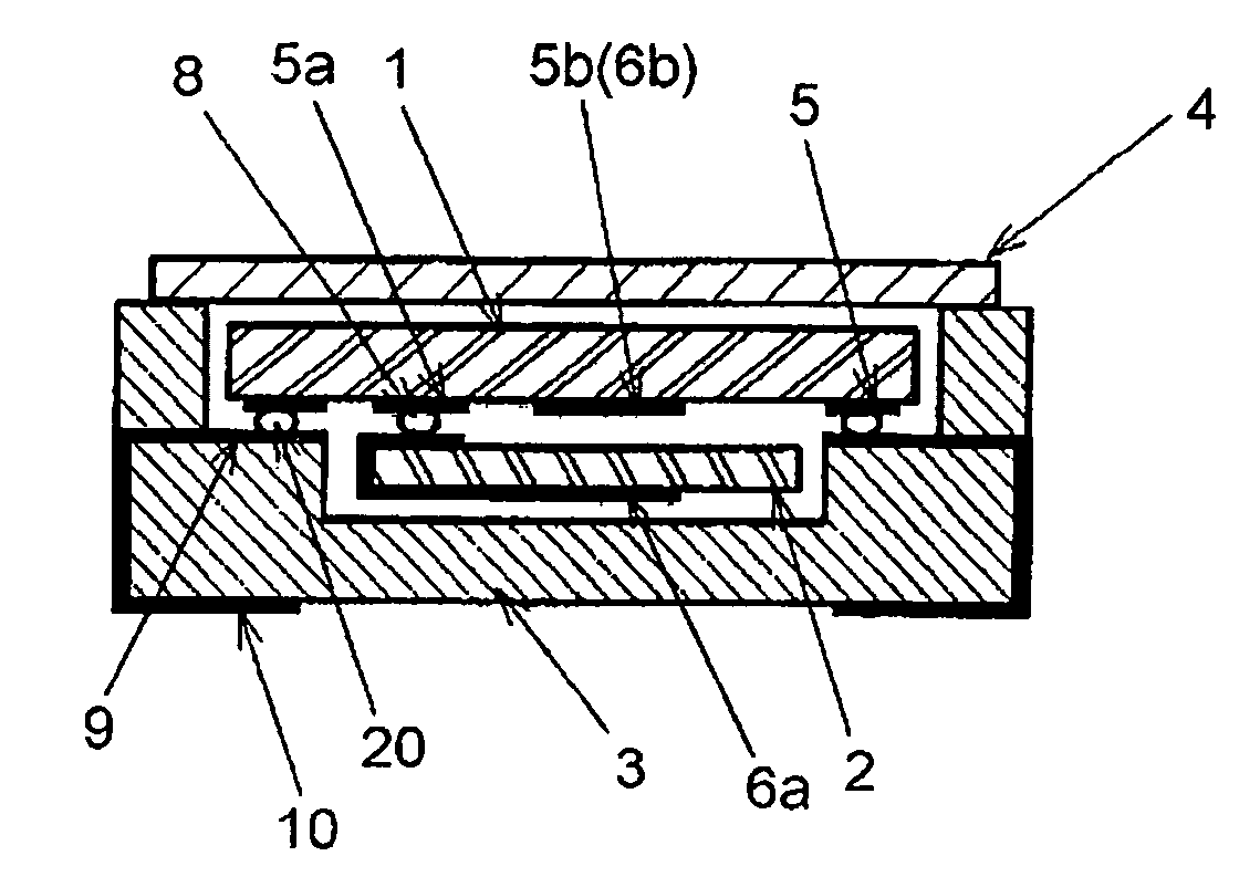
[0043]The surface mount crystal oscillator of the first embodiment comprises surface mount package body 3 similar to the package body in the crystal oscillator illustrated in FIG. 1; IC chip 1 and crystal blank 2 integrated and contained in a recess of package body 3; and a cover 4 put on package body 3 to hermetically encapsulate IC chip 1 and crystal blank 2.

[0044]IC chip 1 has an oscillation circuit, which uses crystal blank 2, and the like integrated therein. On a circuit forming surface of IC chip 1 formed with circuits such as the oscillation circuit, a plurality of IC terminals 5, including a power supply terminal, a ground terminal, and an output terminal, are disposed at four corners of the circuit forming su...

second embodiment

[0061]In the surface mount crystal oscillator of the second embodiment described above, cavity 12 is formed on the other principal surface of crystal blank 2 to ensure the spacing between the vibration region of crystal blank 2 and the back side of IC chip A. Alternatively, the total thickness of crystal connection terminal 5a and eutectic alloy 19 may be controlled, or crystal connection terminal 5a may be increased in thickness, or a spacer may be provided, instead of providing cavity 12. However, the spacing between the vibration region and IC chip 1A can be maintained with certainty when cavity 12 is provided.


PUM


Abstract

In a crystal oscillator having a crystal blank, and an IC chip having integrated therein an oscillation circuit, the crystal blank has a first excitation electrode disposed on its first principal surface, and an extension electrode extended from the first excitation electrode to a peripheral region of the crystal blank, and folded back to the second principal surface. A first and a second crystal connection terminal are disposed on a first principal surface of the IC chip, and the second crystal connection terminal extends to a central region on the first principal surface of the IC chip to constitute a second excitation electrode. The extension electrode is secured to the first crystal connection terminal through a bump, such that the second principal surface of the crystal blank opposes the first principal surface of the IC chip, thereby holding the crystal blank in parallel with the first principal surface of the IC chip. The crystal blank is excited by the first and the second excitation electrodes.

Description

BACKGROUND OF THE INVENTION[0001]1. Field of the Invention[0002]The present invention relates to a crystal oscillator of a surface mount type, and more particularly, to a miniature surface mount crystal oscillator which has a crystal blank mounted on an IC (integrated circuit) chip.[0003]2. Description of the Related Art[0004]A crystal oscillator which includes a quartz crystal unit and an oscillation circuit using the crystal unit integrated therein is used as a reference source for the frequency and time in a variety of devices. Particularly, surface mount crystal oscillators are contained in portable electronic devices as a reference source for the frequency and time because of its small size and light weight. In recent years, the oscillation frequency of surface mount crystal oscillators is made increasingly higher, driven by ever widespreading optical communications systems as well, to reach even into a 600 MHz band.[0005]A further reduction in size as well as a higher oscillat...

Claims


Application Information

Patent Timeline
Patent Type & Authority Patents(United States)
IPC IPC(8): H03H9/02H01L41/09H03B5/32
CPCH03B5/32
Inventor OKAZAKI, MASAYOSHIUEHARA, HIROSHIUMEKI, MITOSHIODA, SEIJI
Owner NIHON DEMPA KOGYO CO LTD
Why Eureka
Try Eureka