
Liquid crystal display panel with reduced parasitic impedance

a liquid crystal display panel and parasitic impedance technology, applied in static indicating devices, instruments, non-linear optics, etc., can solve problems such as interference with a storage voltage, heavy cathode ray tubes, and affecting the appearance of liquid crystals, and achieve the effect of reducing the parasitic impedan

Active Publication Date: 2008-03-04
LG DISPLAY CO LTD
View PDF3 Cites 16 Cited by
  • Summary
  • Abstract
  • Description
  • Claims
  • Application Information

AI Technical Summary

Benefits of technology

The patent describes a liquid crystal display with a unique design that allows for improved image quality and reduced power consumption. The display includes an array substrate with a data line and a gate line, as well as first and second storage wiring. A second substrate, which may be a color filter substrate, has a second pixel region that matches the first pixel region. The first storage wiring is located near the edge of the array substrate, while the second storage wiring is located near the edge of the second substrate. This design allows for more efficient use of space and better image quality.

Problems solved by technology

In the past, displays conveyed images and text through bulky, heavy, and expensive cathode ray tubes.
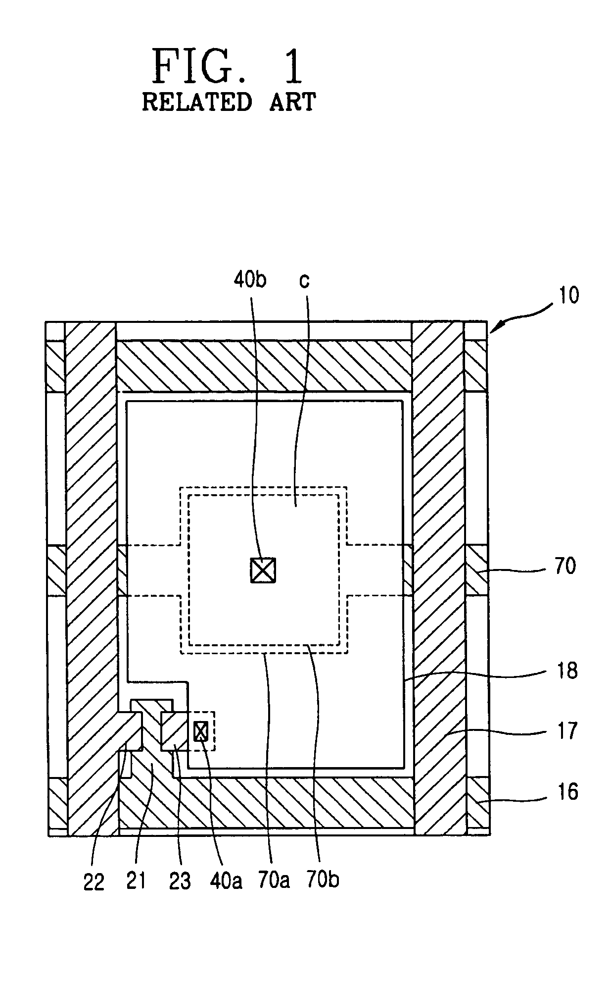
However, this method may cause interference with a storage voltage since it may be coupled to a previous gate signal.
Unfortunately, the properties or characteristics of some liquid crystals may change when a DC voltage is applied for an extended period of time.
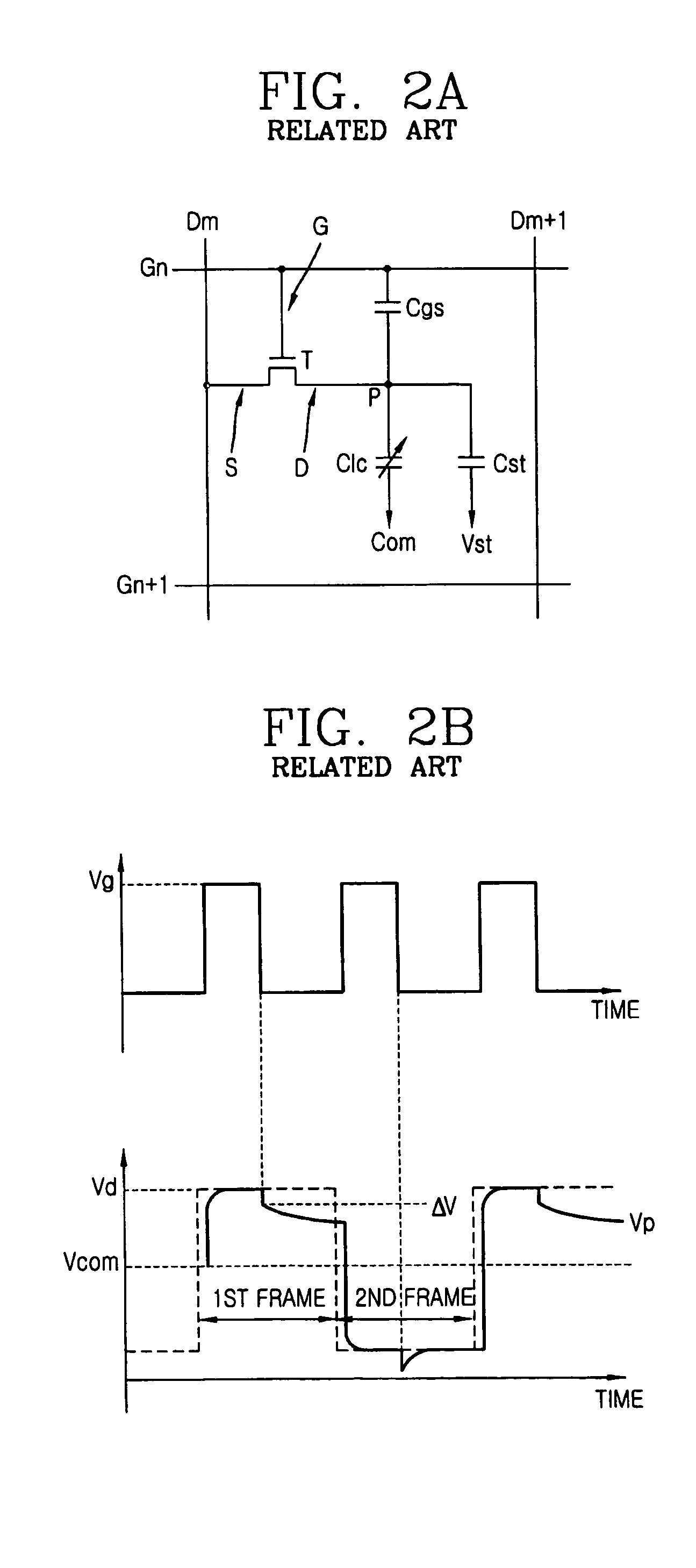
Unfortunately, the reality of the solid line shows that a pixel voltage (Vp) may drop by as much as a kickback voltage (ΔV) in actual liquid crystal display panels.
This condition may cause a screen flicker to occur when an inverted pixel voltage is sourced.
A flicker, an afterimage, or a non-uniform image may occur.
Because of this resistance, signals may become attenuated which may cause image distortions.

Method used


Image

  • Liquid crystal display panel with reduced parasitic impedance
  • Liquid crystal display panel with reduced parasitic impedance
  • Liquid crystal display panel with reduced parasitic impedance

Examples


Embodiment Construction

[0039]A liquid crystal display panel may maintain the voltage that aligns the molecules that make up a liquid crystal layer. By maintaining a constant storage voltage, the liquid crystal display embodiment may minimize flicker, afterimages, and / or other forms of image distortion. By adding storage wiring onto a second substrate, such as a color filter substrate, the continuous length of wire sourcing the storage signal decreases, which decreases the sourced impedance. By reducing the source resistance (e.g., a linear impedance) and / or the capacitive coupling (e.g., a nonlinear impedance) caused by the storage wires, the image quality of the liquid crystal display may improve.

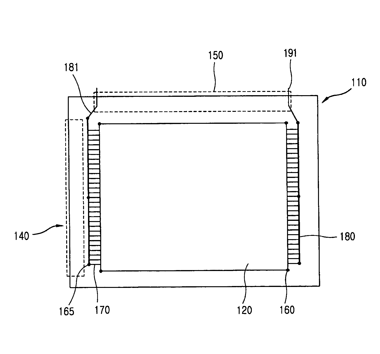
[0040]FIG. 4 is a plan view of a second substrate, such as a color filter substrate 100, which may couple a liquid crystal display. A conductive medium, such as the metal wiring 190 (or a second storage wiring) shown in FIG. 4, is disposed or formed outside of an image-display region of a color filter substrate ...


PUM

PropertyMeasurementUnit
perimeteraaaaaaaaaa
conductiveaaaaaaaaaa
storage voltageaaaaaaaaaa

Abstract

A liquid crystal display includes an array substrate, a data line, a gate line, a first and a second storage wiring, and a second substrate. The data line is disposed on the array substrate and intersects the gate line near a first pixel region. A second substrate, such as a color filter substrate, includes a second pixel region that corresponds to the first pixel region. The first storage wiring is positioned near an edge of the array substrate and the second storage wiring is disposed on the second substrate near an edge of the second substrate.

Description

PRIORITY CLAIM[0001]This application claims the benefit of Korean Patent Application No. P2003-76486 filed in Korea on Oct. 30, 2003. The disclosure of the application is incorporated herein by reference.BACKGROUND[0002]1. Technical Field[0003]The present invention relates to displays, and more particularly to a liquid crystal display panel with a reduced source resistance.[0004]2. Related Art[0005]Displays convey information to viewers. In the past, displays conveyed images and text through bulky, heavy, and expensive cathode ray tubes. Developments in flat panel displays having almost the same display quality as the cathode ray tubes, now convey images through much thinner screens. Further efforts are now being expended to increase the clarity of some flat panel displays images. One such display is a liquid crystal display device.[0006]A liquid crystal display device uses a liquid compound to display images and text by controlling the light transmittance through the liquid compoun...

Claims


Application Information

Patent Timeline
Patent Type & Authority Patents(United States)
IPC IPC(8): G02F1/1343G02F1/133G02F1/1362
CPCG02F1/136213G02F1/136286G02F1/133
Inventor JEOUNG, HUNMOON, SEUNG JUN
Owner LG DISPLAY CO LTD
Learn More