Stacked memory module in mirror image arrangement and method for the same

Active Publication Date: 2008-03-04
TRANSCEND INFORMATION
View PDF3 Cites 6 Cited by
  • Summary
  • Abstract
  • Description
  • Claims
  • Application Information

AI Technical Summary

Benefits of technology

[0007]It is an object of the present invention to provide a method for stacked

Problems solved by technology

However, the signal lines for the stacked memory have non-uniform length and the load impedance might be

Method used


Image

  • Stacked memory module in mirror image arrangement and method for the same
  • Stacked memory module in mirror image arrangement and method for the same
  • Stacked memory module in mirror image arrangement and method for the same

Examples


Embodiment Construction

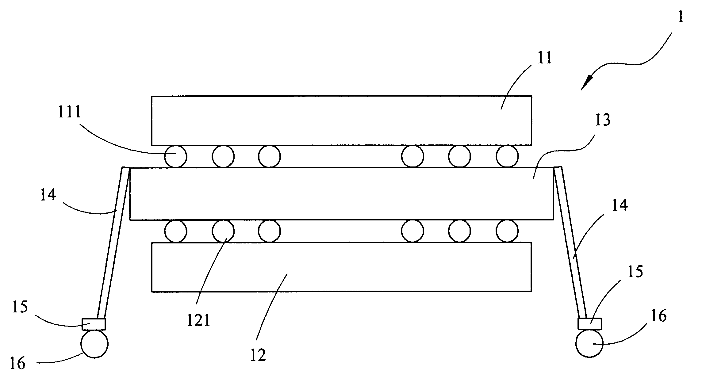
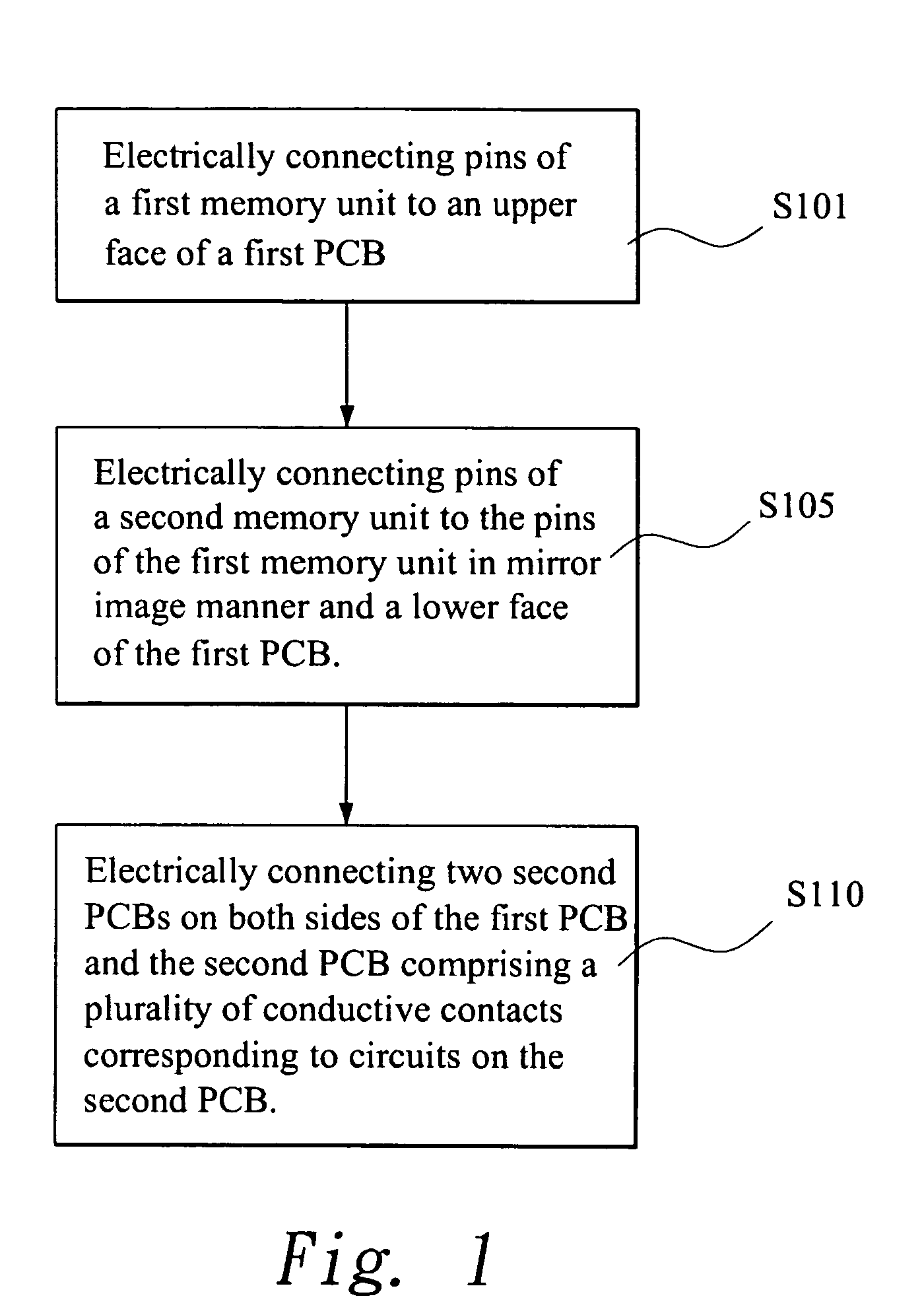
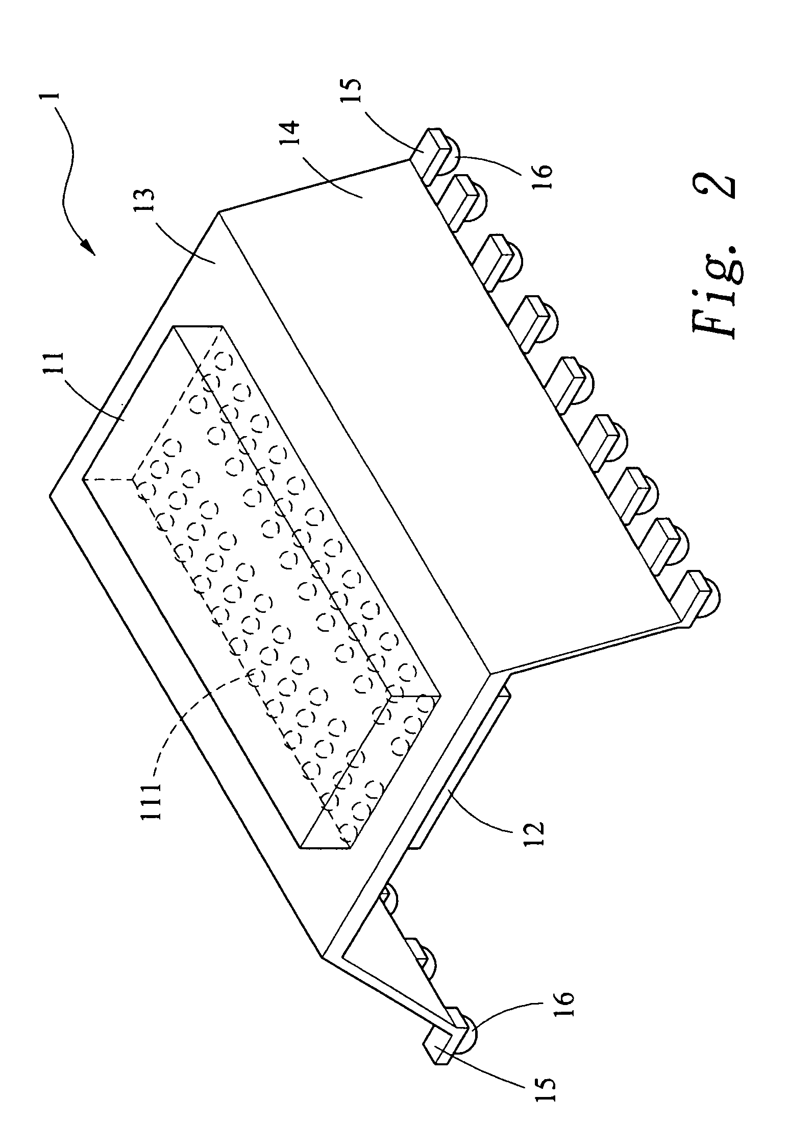
[0020]FIG. 1 shows the flowchart of stacking method for the stacked memory with mirror image structure. In step S101 the pins of a first memory unit are electrically connected to an upper face of a first printed circuit board (PCB), where electronic circuits are arranged on the first PCB. In step S105 a second memory unit is provided with the pins thereof being mirror image to the pins of the first memory unit, where the pins of the second memory unit are arranged on lower face of the first PCB. Therefore, the data of the second memory unit can be sent to the first memory unit through the first PCB.

[0021]In step S110, two second PCBs are electrically connected to both sides of the first PCB, where electronic circuits of the two second PCBs are electrically connected to the electronic circuits of the first PCB for conveying data and signal therebetween. The second PCBs are provided with conductive contacts such as gold finger. The conductive contacts are also electrically connected t...


PUM


Abstract

A stacked memory module is manufactured in mirror image arrangement and a method for the same. The pins of a first memory unit and pins of a second memory unit are electrically connected to an upper face and a lower face of a first printed circuit board made of rigid material. The pins of the second memory unit are in mirror image arrangement with respect to the pins of the first memory unit. Two second PCBs are made of flexible material and electrically connected to both sides of the first PCB. Conductive contacts such as gold fingers are electrically connected to circuit on the second PCB. The manufacture cost is reduced and manufacture process is simplified. The signal quality is enhanced because the signal paths are uniform and the load impedance is reduced.

Description

BACKGROUND OF THE INVENTION[0001]1. Field of the Invention[0002]The present invention relates to a stacked memory module in mirror image arrangement and method for the same, especially to a stacked memory module with two memory units on upper face and lower face of a rigid printed circuit board and two flexible printed circuit board on both sides of the rigid printed circuit, and method for the same.[0003]2. Description of the Prior Art[0004]The processing speed of computer device increases as the progress of technology. The performance of memory is important beside the processing speed of CPU. The conventional computer memory modules generally comprise a plurality of memory units (memory ICs) arranged on carrier (such as printed circuit board) in array fashion. The development trend for memory module is compact and lightweight.[0005]Multi-layer stacked memory module is a design for compact size and high capacity. Taiwan patent gazette No. 091123613 and No. 091221281 disclose that a...

Claims


Application Information

Patent Timeline
IPC IPC(8): H05K7/00
CPCG11C5/02H05K1/147H05K1/141H05K1/189H05K3/363H05K3/4691H05K2201/09172H05K2201/10159H05K2201/10689H05K2201/10734H05K2203/041H05K2203/1572
Inventor WANG, WEI-HSIANGFANG, WEN-JENG
Owner TRANSCEND INFORMATION
Why Eureka
Try Eureka