CMOS imager with Cu wiring and method of eliminating high reflectivity interfaces therefrom

a technology of cu wiring and imager, applied in the field of new cmos (complementary metal oxide semiconductor) image sensor array structure, can solve problems such as degrading device sensitivity

Active Publication Date: 2008-03-11
SMARTSENS TECH (HK) CO LTD
View PDF19 Cites 24 Cited by
  • Summary
  • Abstract
  • Description
  • Claims
  • Application Information

AI Technical Summary

Benefits of technology

[0008]It thus an object of the invention to provide an image sensor having Copper (Cu) metallization levels allowing for incorporation of a thinner interlevel dielectric stack to result in a pixel array exhibiting increased light sensitivity. Improved photosensitivity is possible due to simple geometry; as the height is reduced, the amount of light that arrives in the correct pixel is higher for any given angle.
[0009]It is a further object of the invention to resolve the refractive index mismatch problem caused by the provision of additional Copper metal passivation layers, and, at the same time, increase the sensitivity of the optical image sensors by optimizing the thickness of the dielectric layers under the lenses.
[0010]It a further object of the invention to provide a method of fabricating an image sensor having Copper (Cu) metallization levels that allow for incorporation of a thinner interlevel dielectric stack to result in a pixel array exhibiting increased light sensitivity.

Problems solved by technology

However, as passivation layers provide a refractive index mismatch, their presence will tend to reflect light in the optical path of the pixel cell thus degrading device sensitivity.

Method used


Image

  • CMOS imager with Cu wiring and method of eliminating high reflectivity interfaces therefrom
  • CMOS imager with Cu wiring and method of eliminating high reflectivity interfaces therefrom
  • CMOS imager with Cu wiring and method of eliminating high reflectivity interfaces therefrom

Examples


first embodiment

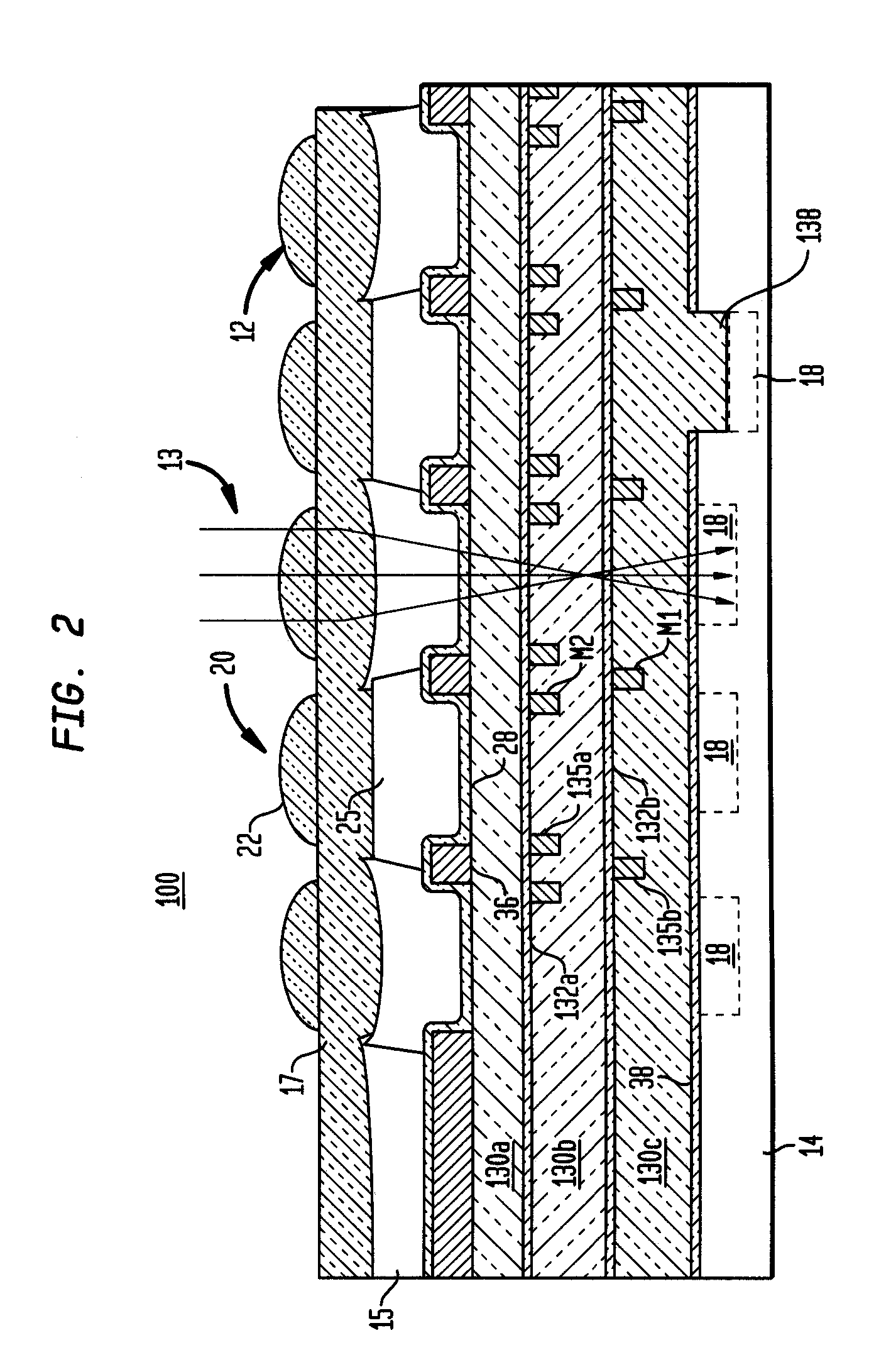
[0043]FIG. 2 illustrates, through a cross-sectional view, a back end of line image sensor array stack 100 according to the invention. While the upper light receiving portion of the pixels 20 (microlens and color filters) are the same as the prior art depicted in FIG. 1, the invention includes the formation of Cu metallization interconnects M1, M2 allowing for the formation of thinner stack of interlevel dielectric layers 130a-130c formed on the substrate 14. The substrate 14 may be a bulk semiconductor including, for example, Si, SiGe, SiC, SiGeC, GaAs, InP, InAs and other III-V compound semiconductors, II-V compound semiconductors, or layered semiconductors such as silicon-on-insulators (SOI), SiC-on-insulator (SiCOI) or silicon germanium-on-insulators (SGOI). Preferably, the interlevel dielectric material may comprise an organic or inorganic interlevel dielectric (ILD) material which may be deposited by any of number of well known techniques such as sputtering, spin-on, or PECVD a...

second embodiment

[0046]Thus, in an alternate second embodiment of pixel array 100b depicted in FIG. 3(b), for the embodiment including STI isolation dielectric regions 138 formed on top of the light sensitive element, e.g., photodiode 18, it is advantageous to remove the substrate capping layer 38 in the optical path on top of the substrate 14 image sensor array 100a in addition to the M1 and M2 level dielectrics 132a,b in the optical path. Thus, in the manner described herein with respect to FIG. 3(a), an additional mask is required and additional lithographic patterning and etching steps (wet or dry etch) implemented to provide additional openings 50a in the SiN capping layer 38 at the locations of the pixel's optical path.

third embodiment

[0047]FIG. 4(a) illustrates, through a cross-sectional view, the image sensor array 100c according to the invention which corresponds to the image sensor embodiment depicted in FIG. 3(a) without the STI regions 138 above the pixel's light sensitive element (photodiode) 18 in the substrate 14. According to this embodiment, the substrate capping layer 38, interlevel dielectric layer 130a, interlevel metallization 135b (M1) and corresponding barrier layer 132b, e.g., SiN, are formed without the M1 barrier etching. Then, the M2 dielectric layer 130b, metallization M2 135a and corresponding barrier layer 132a, e.g., SiN, are formed. A mask is subsequently patterned and an etch is conducted to create an opening 51 to remove that portion of the Nitride barriers 132a for the M2 layer from the pixels' optical paths. However, in the same etch process step, the M2 dielectric layer 130b and the M1 barrier opening 51a is created so that the only one mask is needed to remove both metallization ba...


PUM


Abstract

An image sensor and method of fabrication wherein the sensor includes Copper (Cu) metallization levels allowing for incorporation of a thinner interlevel dielectric stack to result in a pixel array exhibiting increased light sensitivity. The image sensor includes structures having a minimum thickness of barrier layer metal that traverses the optical path of each pixel in the sensor array or, that have portions of barrier layer metal selectively removed from the optical paths of each pixel, thereby minimizing reflectance. That is, by implementing various block or single mask methodologies, portions of the barrier layer metal are completely removed at locations of the optical path for each pixel in the array. In a further embodiment, the barrier metal layer may be formed atop the Cu metallization by a self-aligned deposition.

Description

CROSS REFERENCE TO RELATED APPLICATIONS[0001]The present invention is related to commonly-owned co-pending U.S. patent application Ser. No. 10 / 904,807, filed Nov. 30, 2004 and entitled A DAMASCENE COPPER WIRING IMAGE SENSOR, the whole contents and disclosure of which is incorporated by reference as if fully set forth herein.FIELD OF THE INVENTION[0002]The present invention relates to semiconductor image sensors, and particularly, to a novel CMOS (complementary metal oxide semiconductor) image sensor array structure exhibiting reduced reflectivity and increased light sensitivity, and a process for manufacturing such image sensor array.DESCRIPTION OF THE PRIOR ART[0003]CMOS image sensors are beginning to replace conventional CCD sensors for applications requiring image pick-up such as digital cameras, cellular phones, PDA (personal digital assistant), personal computers, and the like. Advantageously, CMOS image sensors are fabricated by applying present CMOS fabricating process for se...

Claims


Application Information

Patent Timeline
Patent Type & Authority Patents(United States)
IPC IPC(8): H01L31/062
CPCH01L27/14625H01L27/14629H01L27/14636H01L27/14645H01L27/14683H01L21/76819H01L21/76834H01L27/14621H01L27/14627H01L27/146
Inventor ADKISSON, JAMES W.GAMBINO, JEFFREY P.JAFFE, MARK D.LEIDY, ROBERT K.RASSEL, RICHARD J.STAMPER, ANTHONY K.
Owner SMARTSENS TECH (HK) CO LTD
Why Eureka
Try Eureka