Program and program verify operations for flash memory

a technology of flash memory and verification operations, applied in the direction of static storage, digital storage, instruments, etc., can solve the problems of limiting the speed at which cells may be programmed and erased, and limiting the rapid reduction of device siz

Active Publication Date: 2008-03-11
VALLEY DEVICE MANAGEMENT
View PDF8 Cites 18 Cited by
  • Summary
  • Abstract
  • Description
  • Claims
  • Application Information

AI Technical Summary

Benefits of technology

[0009]Yet another aspect of the invention is directed to a method for programming a page of memory cells configured as an array, where each page includes a plurality of subgroups, and each memory cell includes a substrate, a control gate, a charge storage element having two charge storage areas, a source region, and a drain region. The method may include receiving a program command designat...

Problems solved by technology

Unfortunately, the individually addressable nature of conventional NOR flash memory cells tends to lim...

Method used


Image

  • Program and program verify operations for flash memory
  • Program and program verify operations for flash memory
  • Program and program verify operations for flash memory

Examples


Embodiment Construction

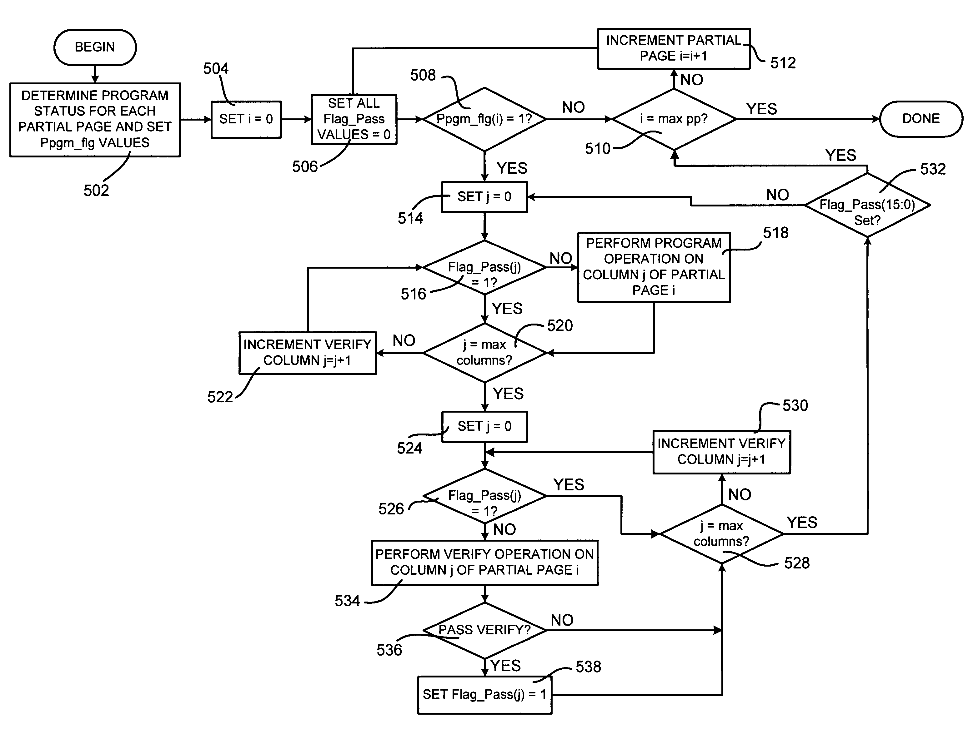
[0016]Techniques described below relate to a flash memory writing technique in which memory cells may be programmed and verified as a page or as a partial page. Registers may be implemented to facilitate more rapid programming and verification.

Memory Device Overview

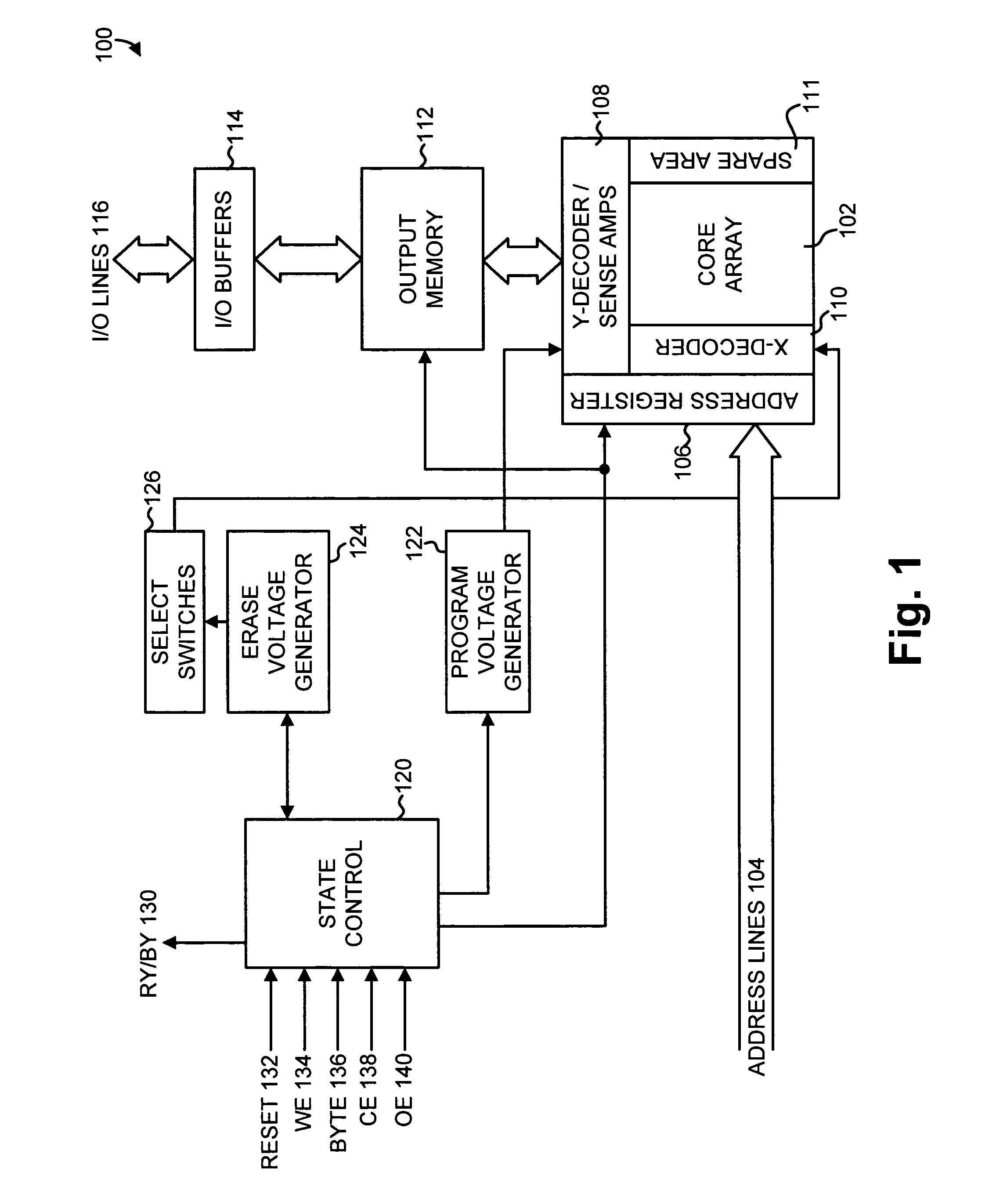
[0017]FIG. 1 is a block diagram illustrating an exemplary high-level implementation of a memory device 100. Memory device 100 may be a Flash memory device implemented as an integrated circuit.

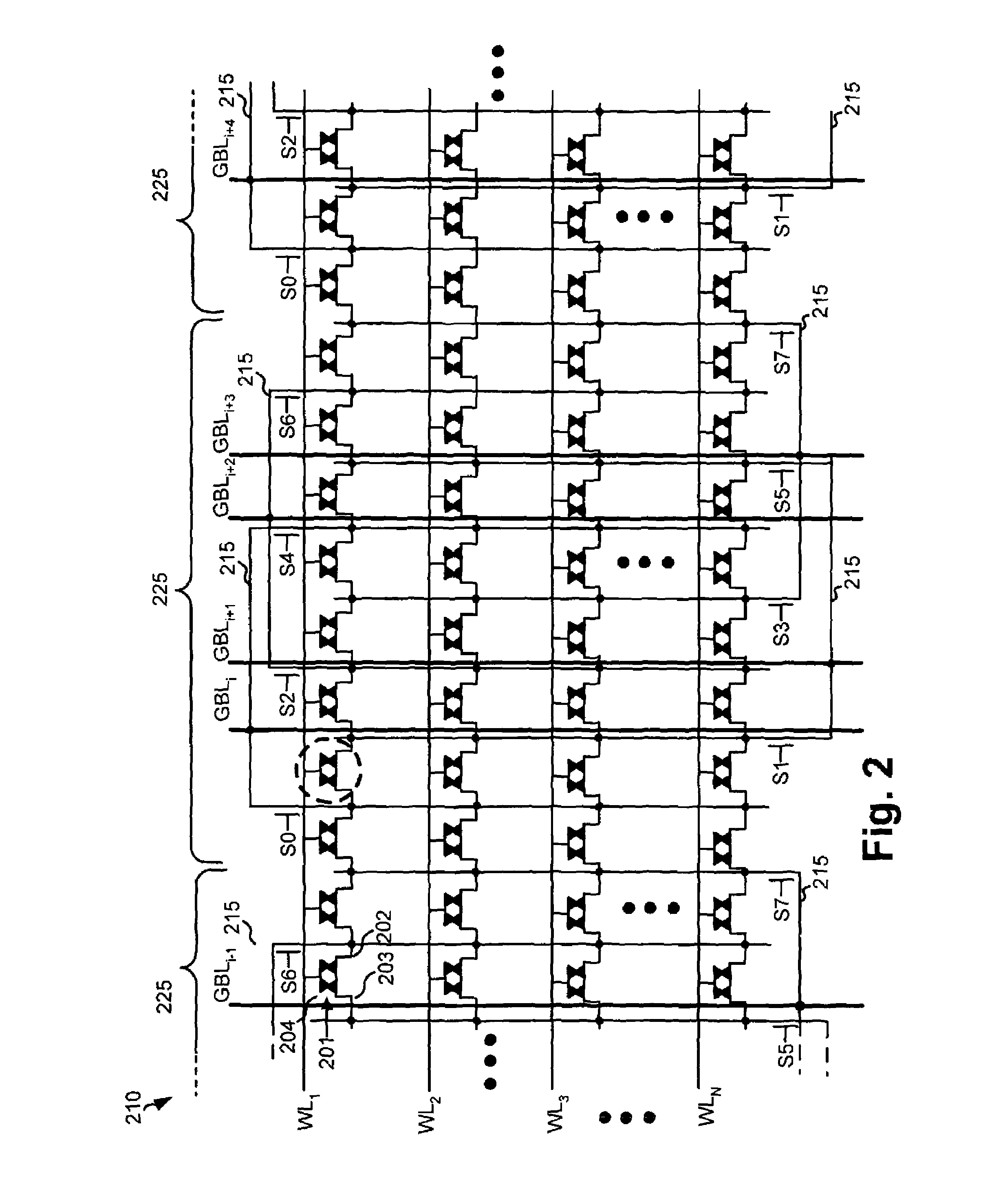
[0018]As shown in FIG. 1, memory device 100 includes a core array 102. Core array 102 may include arrays of high density memory cells, such as, for example, SONOS-type (silicon-oxide-nitride-oxide-silicon) NOR memory cells, where the nitride layer acts as the charge storage element. More specifically, core array 102 may include multiple M×N memory arrays of substantially identical memory cells. As will be discussed in more detail below, core array 102 may be a sequential access memory in which cells' data may be accessed in designate...


PUM


Abstract

A method for programming a nonvolatile memory array including an array of memory cells, each memory cell including a substrate, a control gate, a charge storage element, a source region and a drain region, includes performing a program operation on a group of memory cells, where the group of memory cells includes a plurality of subgroups. A verify status value is stored for each subgroup, the verify status value indicating a verify status of each subgroup, wherein the verify status value indicates whether an associated subgroup has been program verified. A program verify operation is performed on a selected subgroup when the verify status value associated with the selected subgroup indicates that the selected verify subgroup has not been program verified.

Description

TECHNICAL FIELD[0001]The invention relates generally to non-volatile memory devices, and more specifically, to data programming operations for non-volatile memory devices.BACKGROUND ART[0002]Flash memory is a common type of non-volatile semiconductor memory device. Non-volatile refers to the trait of retaining stored data when power is turned off. Because flash memory is non-volatile, it is commonly used in power conscious applications, such as in battery powered cellular phones, personal digital assistants (PDAs), and in portable mass storage devices such as memory sticks.[0003]Flash memory devices typically include multiple individual components formed on or within a substrate. Such devices often comprise a high density section and a low density section. For example, a flash memory may include one or more high density core regions and a low density peripheral portion formed on a single substrate. The high density core regions typically include arrays of individually addressable, s...

Claims


Application Information

Patent Timeline
IPC IPC(8): G11C11/34
CPCG11C16/0475G11C16/3454G11C16/3459
Inventor CHEN, HOUNIENLEONG, NANCY S.
Owner VALLEY DEVICE MANAGEMENT
Why Eureka
Try Eureka