Memory interleave system

a memory interleave and memory technology, applied in the field of memory interleave system, can solve the problems that the conventional memory interleave system cannot improve the performance degradation, and achieve the effect of preventing memory bank contention and improving memory throughpu

Inactive Publication Date: 2008-03-18
NEC CORP
View PDF12 Cites 44 Cited by
  • Summary
  • Abstract
  • Description
  • Claims
  • Application Information

AI Technical Summary

Benefits of technology

[0007]It is an object of the present invention to provide a memory interleave system which can prevent memory bank contention between memory requests by interleaving memory banks, thereby improving memory throughput.

Problems solved by technology

The conventional memory interleave system, however, cannot improve deterioration in performance due to memory bank contention between the memory requests issued by a plurality of CPUs.

Method used


Image

  • Memory interleave system
  • Memory interleave system
  • Memory interleave system

Examples


first embodiment

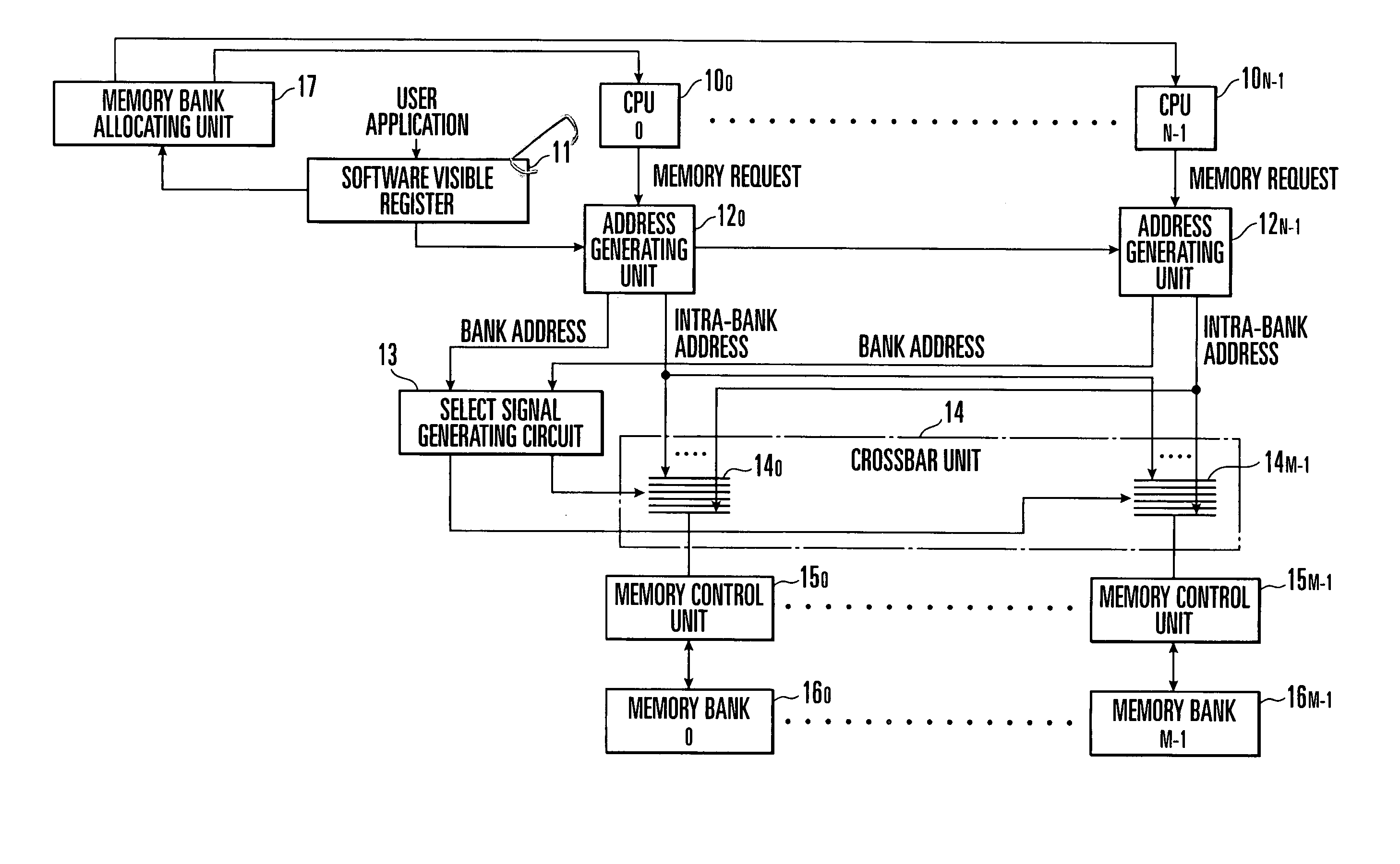
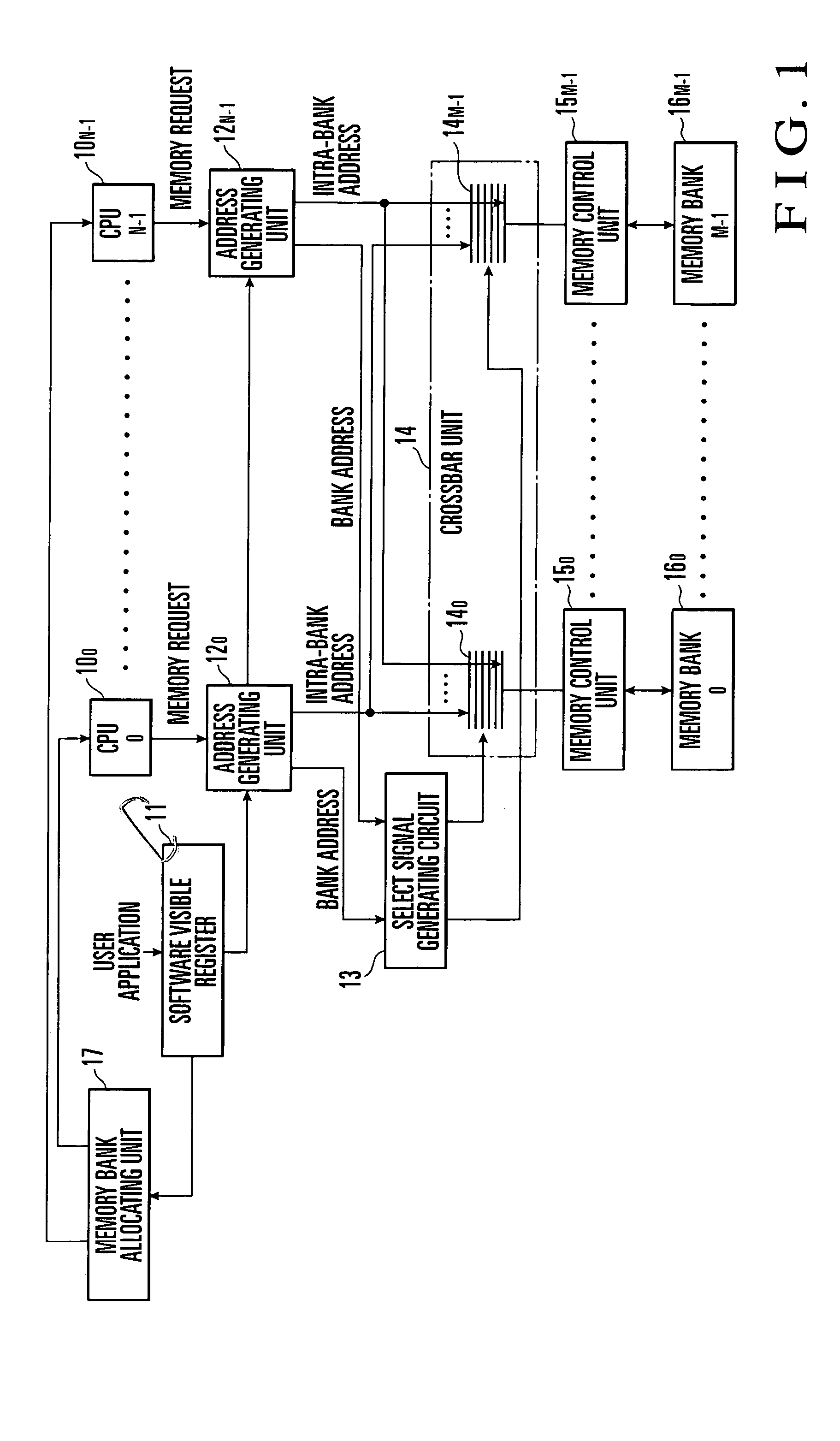
[0016]FIG. 1 shows the arrangement of a memory interleave system according to the first embodiment of the present invention. The memory interleave system according to the first embodiment is comprised of N (a natural number) CPUs (computing means) 100 to 10N-1, a software visible register 11, N address generating units 120 to 12N-1 connected to the CPUs 100 to 10N-1 in a one-to-one correspondence, a select signal generating circuit 13, a crossbar unit 14 comprised of M (M is 2p0 where p is an integer equal to or more than two) selectors 140 to 14M-1, M memory control units 150 to 15M-1 connected to the selectors 140 to 14M-1 in a one-to-one correspondence, M memory banks 160 to 16M-1 connected to the memory control units 150 to 15M-1 in a one-to-one correspondence, and a memory bank allocating unit 17. Note that “N” represents the number of connected CPUs (the number of input ports), and “M” represents the number of connected memory banks. In addition, in the first embodiment, p is ...

second embodiment

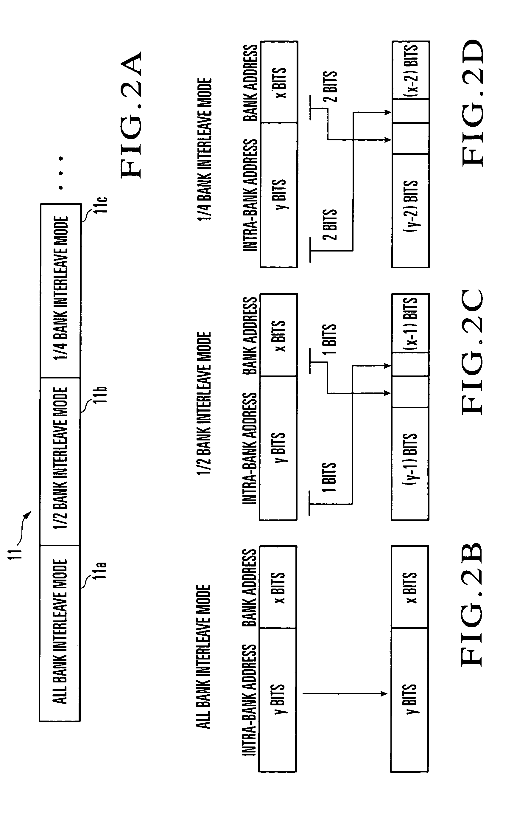
[0051]FIG. 4 shows the arrangement of a memory interleave system according to the second embodiment of the present invention. In the memory interleave system according to the first embodiment shown in FIG. 1, a user application sets a value indicating a bank interleave mode in the software visible register 11. That is, the user application determines a bank interleave mode. In contrast to this, in the memory interleave system according to the second embodiment, a memory bank allocating unit 17 sets a value in a software visible register 11.

[0052]Note that since other portions of which no mention is particularly made are configured in the same manner as corresponding portions in the interleave system according to the first embodiment, they are denoted by the same reference numerals, and a detailed description thereof will be omitted.

[0053]In the memory interleave system according to the second embodiment having the above arrangement, when assigning jobs to be executed to CPUs 100 to ...

third embodiment

[0056]FIG. 5 shows the arrangement of a memory interleave system according to the third embodiment of the present invention. In the memory interleave systems according to the first and second embodiments shown in FIGS. 1 and 4, a bank interleave mode is determined by setting a value indicating a bank interleave mode in the software visible register 11. In contrast to this, in the memory interleave system according to the third embodiment, a user determines a bank interleave mode by manually setting a value indicating a bank interleave mode with a hardware switch 21 such as a dip switch.

[0057]Note that since other portions of which no mention is particularly made are configured in the same manner as corresponding portions in the interleave system according to the first embodiment, they are denoted by the same reference numerals, and a detailed description thereof will be omitted.

[0058]In the memory interleave system according to the third embodiment having the above arrangement, the ...


PUM


Abstract

A memory interleave system includes M (M=2p, where p is a natural number) memory banks, M memory control units (MCU) corresponding respectively to the M memory banks, N (a natural number) CPUs, and N address generating units (AGU) corresponding respectively to the N CPUs. Each memory bank includes a plurality of memories. The CPUs output memory requests, each containing a first bank address (address of the memory bank) and a first intra-bank address (address of a memory in the memory bank). Each AGU receives a memory request from a corresponding CPU, and generates and outputs a second intra-bank address and a second bank address by using the first intra bank address and the first bank address. Each memory control MCU performs memory bank access control on the basis of the second intra-bank address. An MCU performing access control is selected on the basis of the second bank address.

Description

BACKGROUND OF THE INVENTION[0001]The present invention relates to a memory interleave system which realizes efficient memory access in a computer system.[0002]FIG. 6 shows an example of the arrangement of a conventional memory interleave system.[0003]The conventional memory interleave system shown in FIG. 6 is comprised of a vector computing unit (CPU) 101 which outputs eight vector elements V0 to V7, a leading element address, and an inter-element distance and generates a memory request for each vector element, a main storage unit 102 comprised of a plurality of memory banks 121, and a memory access control unit 103 which independently performs access control on each memory bank 121 between the vector computing unit 101 and the main storage unit 102 on the basis of a memory request.[0004]The memory access control unit 103 further includes an adder unit 104, routing address generating unit 105, contention arbitration unit 106, and crossbar unit 107. The adder unit 104 adds the leadi...

Claims


Application Information

Patent Timeline
Patent Type & Authority Patents(United States)
IPC IPC(8): G06F12/00G06F12/06G11C8/12G06F12/02G11C7/00G11C8/00
CPCG06F12/0607G11C7/00G11C8/00G11C8/12
Inventor ISHIKAWA, HISASHI
Owner NEC CORP
Why Eureka
Try Eureka