Apparatus and method for thin-layer metrology

Active Publication Date: 2008-03-25
VISTEC SEMICON SYST JENA
View PDF17 Cites 2 Cited by
  • Summary
  • Abstract
  • Description
  • Claims
  • Application Information

AI Technical Summary

Benefits of technology

[0026]The method according to the present invention likewise offers numerous advantages. Firstly the semiconductor substrates are transported out of at least one cassette element to a measurement unit for thin-layer micrometrology. In this context, the semiconductor substrates are guided along past or beneath the measurement unit for thin-layer macrometrology. As the semiconductor substrates are guided along beneath the measurement unit for thin-layer macrometrology, measurement locations on the semiconductor substrates that indicate defects and must be examined more closely are deter

Problems solved by technology

The apparatus described in the patent has the critical disadvantage, however, that only one specif

Method used


Image

  • Apparatus and method for thin-layer metrology
  • Apparatus and method for thin-layer metrology
  • Apparatus and method for thin-layer metrology

Examples


Embodiment Construction

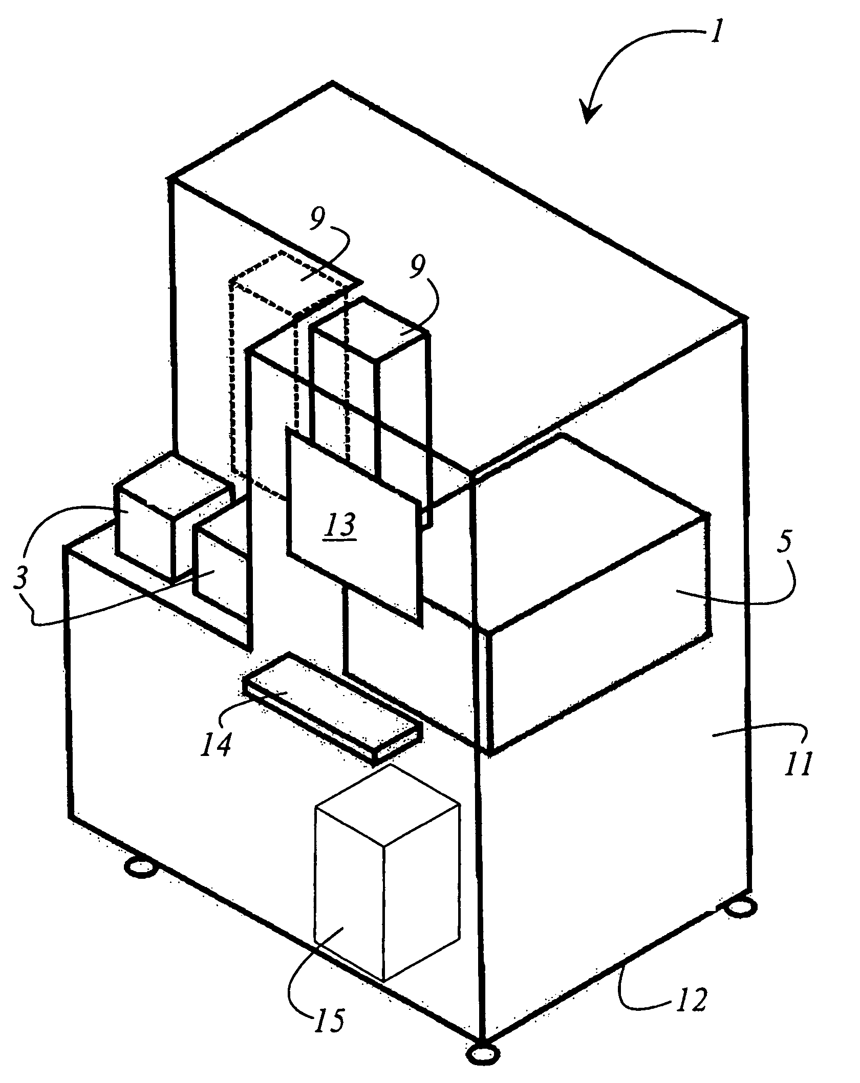
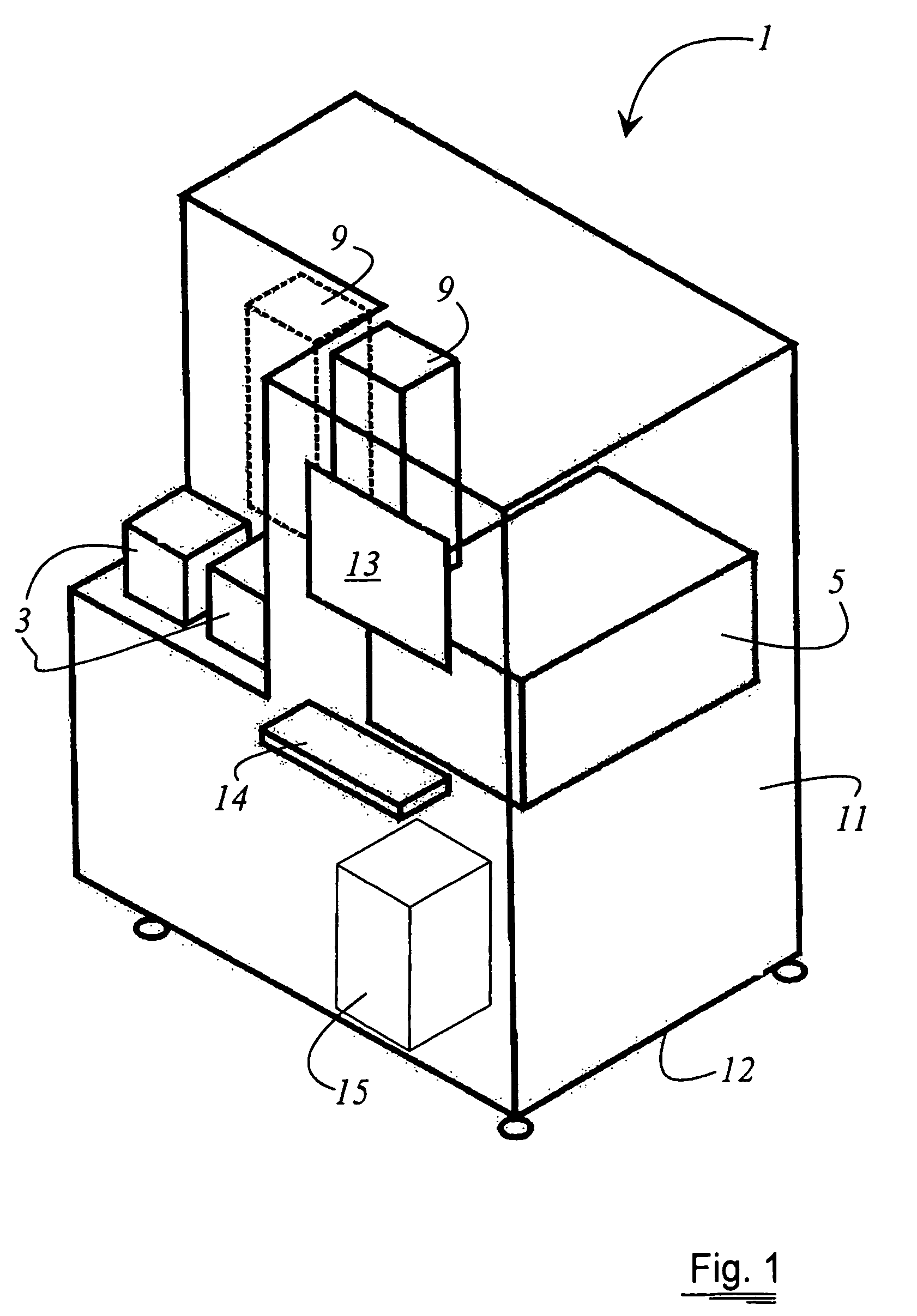
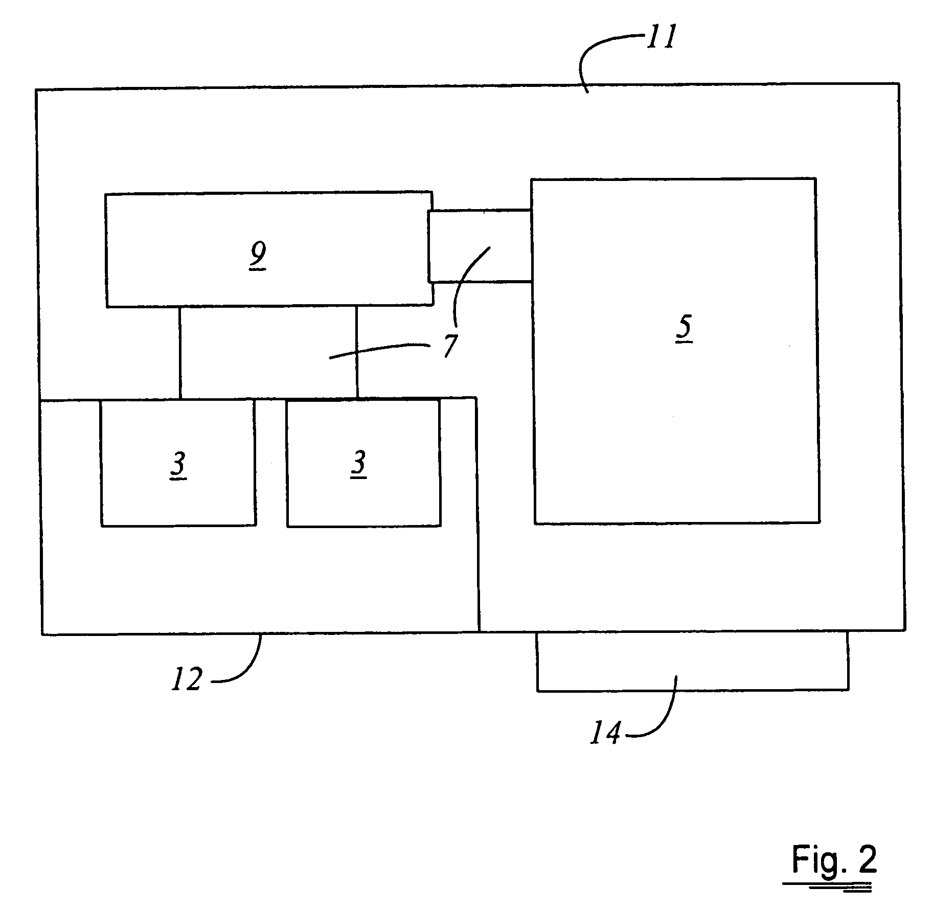
[0034]FIG. 1 is a schematic perspective view of apparatus 1 for thin-layer metrology that combines in a single measurement device the specific advantages of the method for microscopic examination and the method for macroscopic examination. A higher-quality metrology solution is thus available to the user. The Figure shows the principle of the methodology according to the present invention with reference to a device that is typical for 200-mm wafer metrology. No limitations arise therefrom, however, regarding other device forms or variant arrangements, in particular regarding devices that are used for 300-mm wafer metrology. The parts of the device discussed below are then applicable analogously. Apparatus 1 comprises a housing 11 that defines a basal area 12. At least one cassette element 3 is associated with housing 11 of apparatus 1. Semiconductor substrates are introduced via cassette element 3 into apparatus 1 in order to perform the corresponding measurements or examinations on...


PUM


Abstract

An apparatus (1) and a method for thin-layer metrology of semiconductor substrates (16) are disclosed. The semiconductor substrates (16) are delivered or transported to the apparatus (1) by means of at least one cassette element. A measurement unit (5) for thin-layer micrometrology is provided in the apparatus (1), the semiconductor substrates being conveyed by means of a transport mechanism (7) from the cassette element (3) to the measurement unit (5) for thin-layer micrometrology. A measurement unit (9) for thin-layer macrometrology is provided in the region of the transport mechanism (7) after the cassette element (3). By means of the measurement unit (9) for thin-layer macrometrology, measurement locations (22) on the semiconductor substrate that require more detailed examination in the measurement unit (5) for thin-layer micrometrology can rapidly be identified.

Description

CROSS REFERENCE TO RELATED APPLICATIONS[0001]This application claims priority of the German patent application 103 08 258.1 which is incorporated by reference herein.FIELD OF THE INVENTION[0002]The invention concerns an apparatus for thin-layer metrology. The invention concerns in particular an apparatus for thin-layer metrology on semiconductor substrates, the apparatus comprising at least one cassette element for semiconductor substrates and a first measurement unit for thin-layer micrometrology. In addition, a transport mechanism is provided between the cassette element for the semiconductor substrates and the measurement unit for thin-layer micrometrology.[0003]The invention furthermore concerns a method for thin-layer metrology.BACKGROUND OF THE INVENTION[0004]German Patent DE 100 53 232 discloses a substrate delivery module for a workstation. Semiconductor substrates are transferred out of the substrate delivery module to the workstation for further examination. In the worksta...

Claims


Application Information

Patent Timeline
IPC IPC(8): G01B11/28G01B11/02G06K9/00G01B11/04G01B11/06G01N21/00G01B11/08G01N21/956H01L21/00H01L21/66
CPCH01L21/67207H01L21/67253
Inventor SLODOWSKI, MATTHIAS
Owner VISTEC SEMICON SYST JENA
Why Eureka
Try Eureka