Matrix panel display apparatus and driving method therefor wherein auxiliary signals are applied to non-selected picture elements

a technology of matrix panel and display apparatus, which is applied in the direction of instruments, static indicating devices, etc., can solve the problems of non-uniform brightness, waveform distortion of counter electrode voltage and scanning voltage, and amplitude of signal voltage, so as to reduce parasitic capacitance between terminals of tfts and not deteriorate the picture quality, the effect of reducing the parasitic capacitance of the terminals

Inactive Publication Date: 2008-04-08
PANASONIC LIQUID CRYSTAL DISPLAY CO LTD +1
View PDF9 Cites 44 Cited by
  • Summary
  • Abstract
  • Description
  • Claims
  • Application Information

AI Technical Summary

Benefits of technology

[0005]Objectives of the present invention are providing a display apparatus and a drive method in which the signal voltages of the liquid crystal matrix panel are lowered without deteriorating the picture quality, non-uniformity of brightness over the panel caused by non-uniformity of output voltages of the drive circuit and the parasitic capacitances between terminals of TFTs is reduced and smearing in a displayed picture is prevented.

Problems solved by technology

By this method, the amplitudes of signal voltages can be lowered, but the waveform distortion of the counter electrode voltages and the scanning voltage increases, since parasitic capacitances and resistances of the wiring increase due to an increase in the size of the liquid crystal panel.
Therefore, the voltage applied to the liquid crystal changes depending on the pattern displayed on the panel, and a non-uniform brightness and a deterioration of picture quality occurs in the panel thereby.
Especially, in a high resolution liquid crystal panel having about a thousand scanning lines, the influences of the waveform distortion becomes severe and the picture quality deterioration occurs significantly due to a short scanning time of one line.
The storage capacitances and the parasitic capacitances have considerable non-uniformity in the panel when the panel size is as much as 10-15 inches, which is as large as the display panel size of personal computers.
The non-uniformity is induced because the accuracy of photo-mask adjustment and etching in the process of TFT production degrades proportionately as the panel size becomes large.
So the reliability deterioration of the liquid crystal and the of the after-image phenomenon occurrence become more significant as the panel size increases.
These methods do not resolve the problem of poor picture quality, such as the occurrence of a striped picture in the horizontal direction (referred to as smearing).

Method used


Image

  • Matrix panel display apparatus and driving method therefor wherein auxiliary signals are applied to non-selected picture elements
  • Matrix panel display apparatus and driving method therefor wherein auxiliary signals are applied to non-selected picture elements
  • Matrix panel display apparatus and driving method therefor wherein auxiliary signals are applied to non-selected picture elements

Examples


embodiment 1

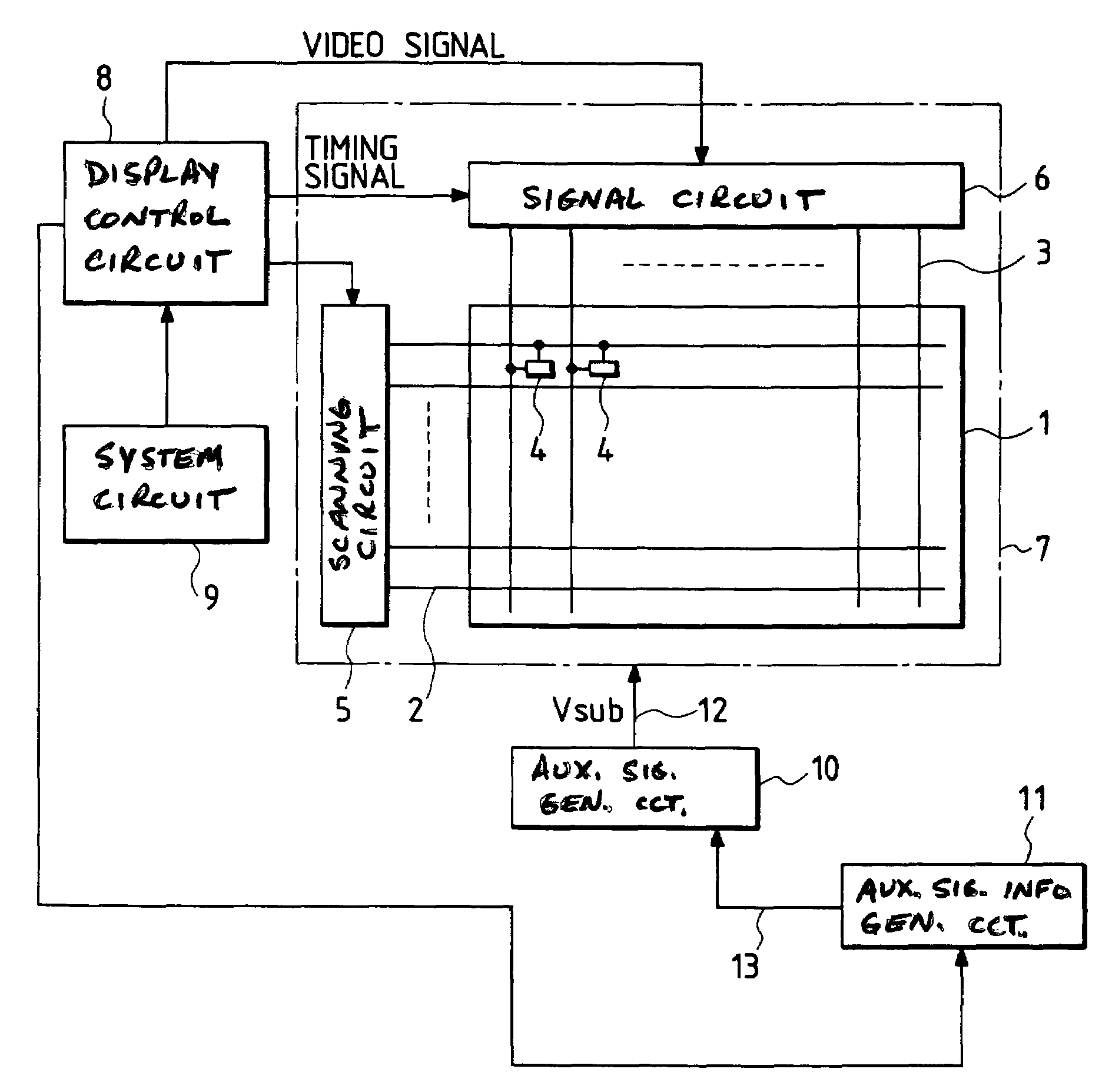
[0041]A conceptual figure of the overall constitution of the display apparatus of the present invention is shown in FIG. 1. The display apparatus comprises a matrix panel 1 consisting of scanning lines 2, signal lines 3 and picture elements 4, provided at the intersection points where the lines 2 and the lines 3 cross each other; a scanning circuit 5 and a signal circuit 6 for generating predetermined voltages and applying them to the scanning lines 2 and the signal lines 3, respectively; a display control circuit 8 for supplying timing signals to the scanning circuit 5 and the signal circuit 6 and an auxiliary signal for increasing the effective value of the signal voltages generating circuit 10; a system circuit 9 connected to the display control circuit 8; the auxiliary signal generating circuit 10; and an auxiliary signal information generating circuit 11 connected to the auxiliary signal generating circuit 10 through an auxiliary signal line 13. As to the picture elements 4, an...

embodiment 2

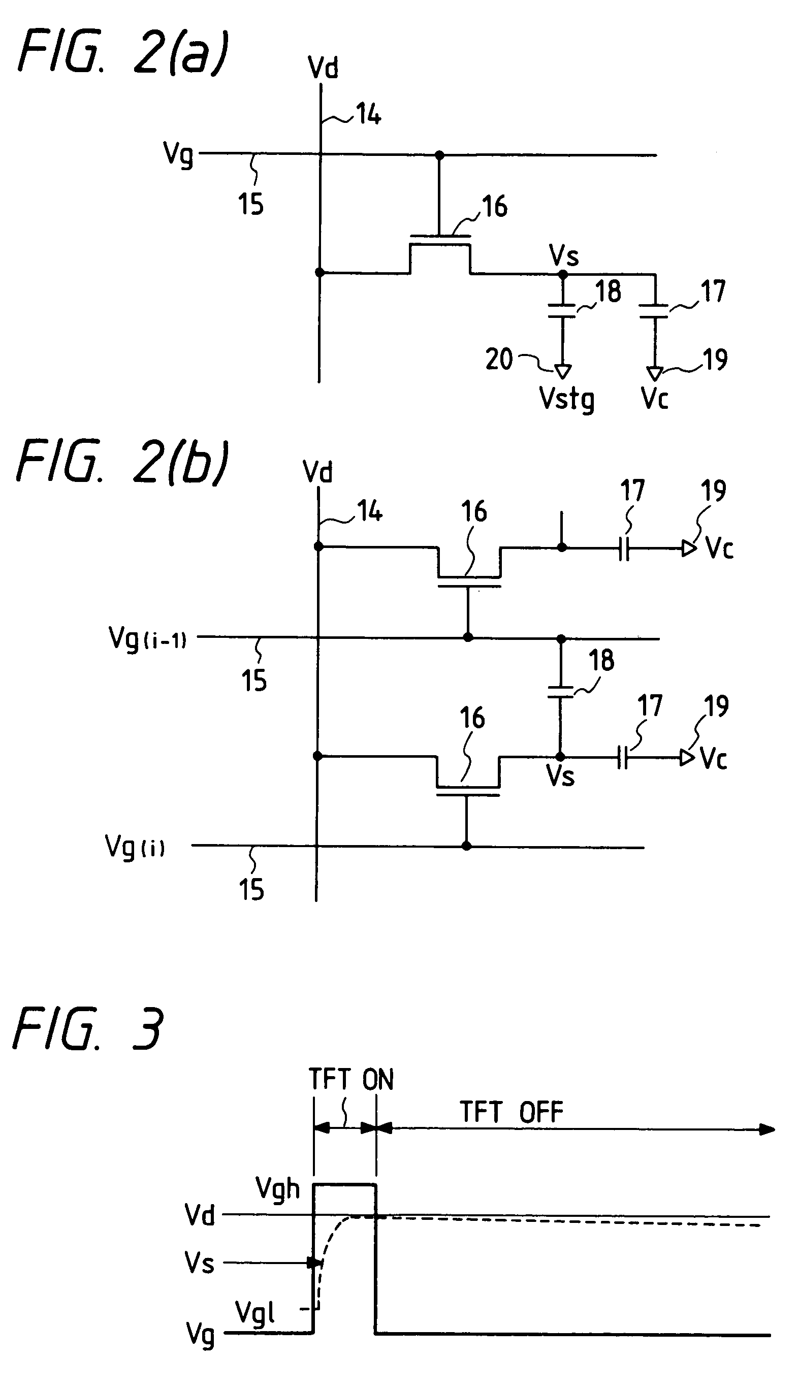
[0044]FIG. 5 shows an embodiment of the present invention in which the equivalent circuit of the picture elements 4 is that of FIG. 2(b). One picture element consists of the TFT 16, the liquid crystal 17 between a picture element electrode and a counter electrode (not shown in the figure) and the storage capacitance 18, and all of the picture elements are arranged as distributed dots of a (m×n) matrix. A terminal of each liquid crystal 17 is connected to a respective TFT 16 and the other terminal of the liquid crystal 17 is connected to the auxiliary signal generating circuit 10. A terminal of each storage capacitance 18 is connected to a respective TFT 16 and the other terminal of the storage capacitance 18 is connected to a scanning line 15, which defers from the embodiment 1. FIG. 7 shows an example of driving timing for the scanning electrodes and the signal electrodes of the liquid crystal matrix panel, which is common to the embodiments 1 and 2. The scanning voltage Vgl-Vgn ar...

embodiment 3

[0046]FIG. 11(a) shows an equivalent circuit of a picture element and FIG. 11(b) is a waveform diagram of the driving timing in another embodiment. The embodiment corresponds to FIG. 2(b), in which one terminal of the storage capacitance is connected to the source terminal S and the other terminal is connected to the scanning line 15 adjoining the scanning line connected to the TFT 16. The auxiliary signal Vsub is applied to the common terminal 19 in the embodiment shown in FIG. 5, having the same equivalent circuit shown in FIG. 2(b); on the other hand, the auxiliary signal is applied through the scanning line 15 in the present embodiment. The auxiliary signal Vsub of an amplitude VCN smaller than the voltage Vgh besides Vgh,Vgl for turning ON or OFF each TFT is applied to the scanning voltage Vg(i). The voltage Vgh, applied as the scanning voltage Vg(i), is transmitted to the source terminal S of the TFT 16 and, synchronizing it, the source voltage Vs is generated. When the source...


PUM


Abstract

A matrix panel display apparatus includes plural signal lines and plural scanning lines intersecting each other and, near each intersection point, a picture element including a picture element electrode, a counter electrode, a display medium disposed between the picture element electrode and the counter electrode, and a transistor for applying image signals from the signal line to the picture element electrode. The transistor is controlled in response to scanning signals received on a scanning line. An auxiliary signal generating circuit generates auxiliary signals for increasing effective voltages of the image signals and applies the auxiliary signals to the picture elements while each of the transistors is in a non-conducting state and each of the picture elements is not selected. Preferably, the auxiliary signal generating circuit applies the auxiliary signals to the picture elements during a predetermined period in which all of the transistors are in the non-conducting state and none of the picture elements is selected.

Description

[0001]This application is a continuation of application Ser. No. 08 / 139,904 filed Oct. 22, 1993 now abandoned.BACKGROUND OF THE INVENTION[0002]The present invention relates to a matrix display apparatus and its driving method; particularly, to a display apparatus and a driving method capable of uniform brightness display, as well as the lowering of signal voltages and power consumption.[0003]One of the important considerations in the design and operation of a liquid crystal display apparatus is the lowering of the driving voltage. Lowering the driving voltage brings about improvement of such factors as picture quality deterioration, non-uniform brightness in the display panel and power consumption reduction. Furthermore, the reliability of circuits in the display apparatus can be improved and a lower price can be realized by downsizing the driving circuits. Especially, in using MOS-LSI techniques in the manufacture of the driving circuit, the price of the display apparatus is lowere...

Claims


Application Information

Patent Timeline
Patent Type & Authority Patents(United States)
IPC IPC(8): G09G3/36
CPCG09G3/3655G09G3/3659G09G3/3677G09G2300/0426G09G2300/0876G09G2310/0224G09G2310/06G09G2320/0219G09G2320/0247G09G2320/041G09G2330/021G09G3/3614G09G3/3696G09G2310/0264G09G2320/0233
Inventor OTA, MASAYUKITSUMURA, MAKOTOKITAJIMA, MASAAKIMISHIMA, YASUYUKIKAKEHI, NAOFUMI
Owner PANASONIC LIQUID CRYSTAL DISPLAY CO LTD
Why Eureka
Try Eureka