

Organic light-emitting diode display device
a light-emitting diode and display device technology, applied in the direction of semiconductor devices, basic electric elements, electrical appliances, etc., can solve the problems of reducing light emission efficiency and lifetime of oled, reducing the uniform thickness of organic light-emitting layers, and reducing the display quality. uniform
- Summary
- Abstract
- Description
- Claims
- Application Information
AI Technical Summary
Benefits of technology
Problems solved by technology
Method used
Image

Examples
first embodiment
[0044]FIG. 3 is a plan view illustrating an OLED according to the present disclosure. FIG. 4A is a cross-sectional view taken along line IVa-IVa of FIG. 3. FIG. 4B is a cross-sectional view taken along line IVb-IVb of FIG. 3.
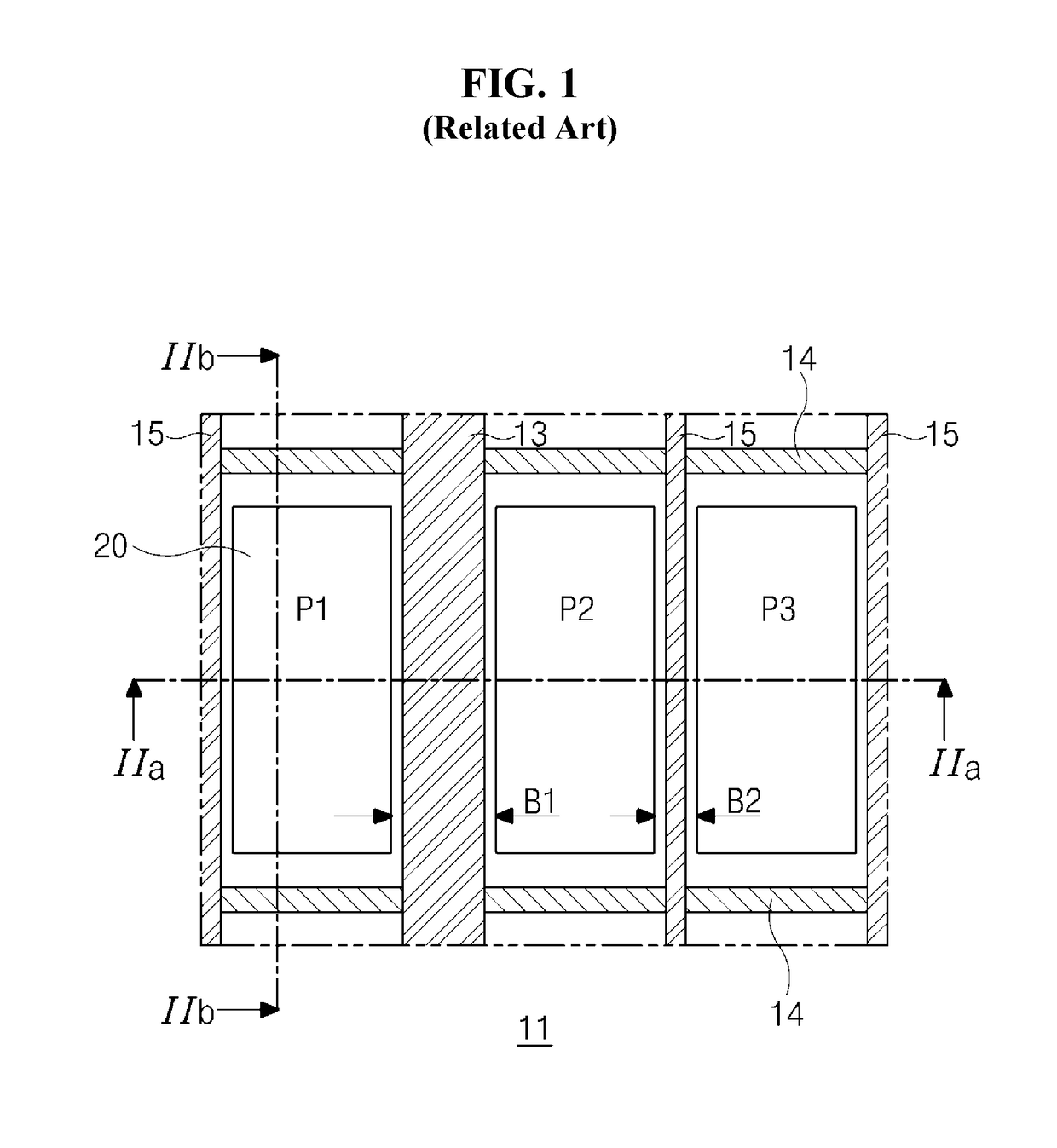
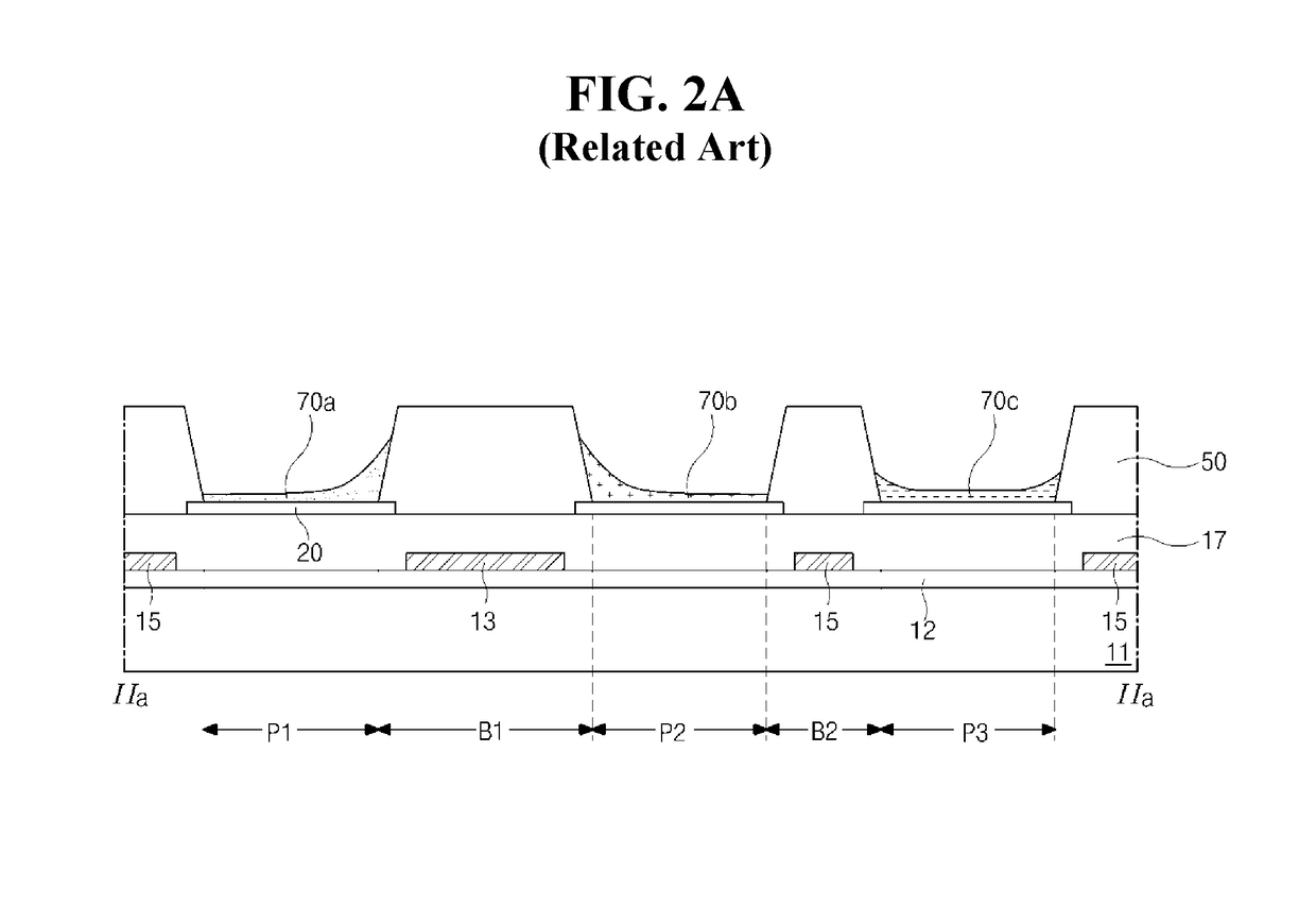
[0045]With reference to FIG. 3, the OLED of the first embodiment may include a substrate 101 including first to third pixel regions P1 to P3 arranged in a horizontal direction, a first electrode 120 in each of first to third pixel regions P1 to P3 on the substrate 101, and a gate line 114, a data line 115, and a power line 113 on the substrate 101. The substrate 101 may include three or more pixel regions. In one example, a fourth pixel region may be arranged at one side of the first to third pixel regions P1 to P3.
[0046]For example, the gate line 114 may be arranged in the horizontal direction at a lower side of the first to third pixel regions P1 to P3. The data line 115 may cross the gate line 114, and may be arranged at each of boundary portions B1 and B2 am...
second embodiment
[0058]FIG. 5 is a plan view illustrating an OLED according to the present disclosure. FIG. 6A is a cross-sectional view taken along line VIa-VIa of FIG. 5. FIG. 6B is a cross-sectional view taken along line VIb-VIb of FIG. 5.
[0059]With reference to FIG. 5, the OLED of the second embodiment may include a substrate 201 including first to third pixel regions P1 to P3 arranged in a horizontal direction, a first electrode 220 in each of first to third pixel regions P1 to P3 on the substrate 201, and a gate line 214, a data line 215, and a power line 213 on the substrate 201. The substrate 201 may include three or more pixel regions. In one example, a fourth pixel region may be arranged at one side of the first to third pixel regions P1 to P3. Further, the OLED may include an auxiliary electrode 221 located at a boundary portion between pixel regions along a vertical direction and spaced apart from the first electrode 220.
[0060]For example, the gate line 214 may be arranged in the horizon...
third embodiment
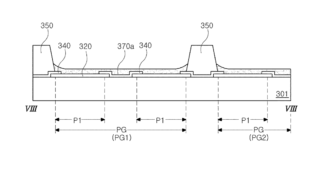
[0075]FIG. 7 is a plan view illustrating an OLED according to the present disclosure. FIG. 8 is a cross-sectional view taken along line VIII-VIII of FIG. 7.
[0076]The OLED of the third embodiment is similar to the OLED of the first or second embodiments, except for a structure of pixel regions emitting the same color on each column line. Explanations similar to parts of the first or second embodiment may be omitted. For the purpose of explanation, gate lines, data lines, and power lines, and so on are not shown in FIGS. 7-8.
[0077]In the OLED of this embodiment, pixel regions emitting the same color may be located on each column line. For example, the first pixel regions P1 on the first column line may emit red, the second pixel regions P2 on the second column line may emit green, and the third pixel regions Ps on the third column line may emit blue. Embodiments are not limited thereto. The first pixel region P1, the second pixel region P2, and the third pixel region P3 may alternate ...
PUM
 Abstract
Description
Claims
Application Information