Feedback control of chemical mechanical polishing device providing manipulation of removal rate profiles

a technology of chemical mechanical polishing and feedback control, which is applied in the direction of total factory control, programme control, lapping machines, etc., can solve the problems of exacerbate process-induced variations, the wafer surface coming into the cmp process may be non-uniform, and the process may drift from its optimized state, so as to improve the uniformity of the thickness of the wafer, improve the run-to-run control of the wafer thickness profile, and enhance the effect of process results

Inactive Publication Date: 2007-05-10
APPLIED MATERIALS INC
View PDF99 Cites 30 Cited by
  • Summary
  • Abstract
  • Description
  • Claims
  • Application Information

AI Technical Summary

Benefits of technology

[0009] The present invention relates to a method, apparatus and medium for planarizing a surface of a substrate, for example, a semiconductor wafer, in order to improve run-to-run control over the wafer thickness profile. The present invention uses a model (which can be implemented as a single model or multiple models) of the planarization process to predict material removal across the wafer surface and to improve within wafer thickness uniformity. Deviations from the predicted outcome are used to set new polishing parameters, which feedback into the process to enhance process results.

Problems solved by technology

Typically, the CMP device is optimized for a particular process, but because of chemical and mechanical changes to the process, e.g., changes in the polishing pad during polishing, degradation of process consumables, and other factors, the CMP process may drift from its optimized state.
In addition to processing drift, the wafer surface coming into the CMP process may be non-uniform, which exacerbates the process-induced variations across the post-polished surface.
However, these schemes are still not adequate in today's manufacturing environment to satisfactorily compensate for the aforementioned effects.

Method used


Image

  • Feedback control of chemical mechanical polishing device providing manipulation of removal rate profiles
  • Feedback control of chemical mechanical polishing device providing manipulation of removal rate profiles
  • Feedback control of chemical mechanical polishing device providing manipulation of removal rate profiles

Examples


Embodiment Construction

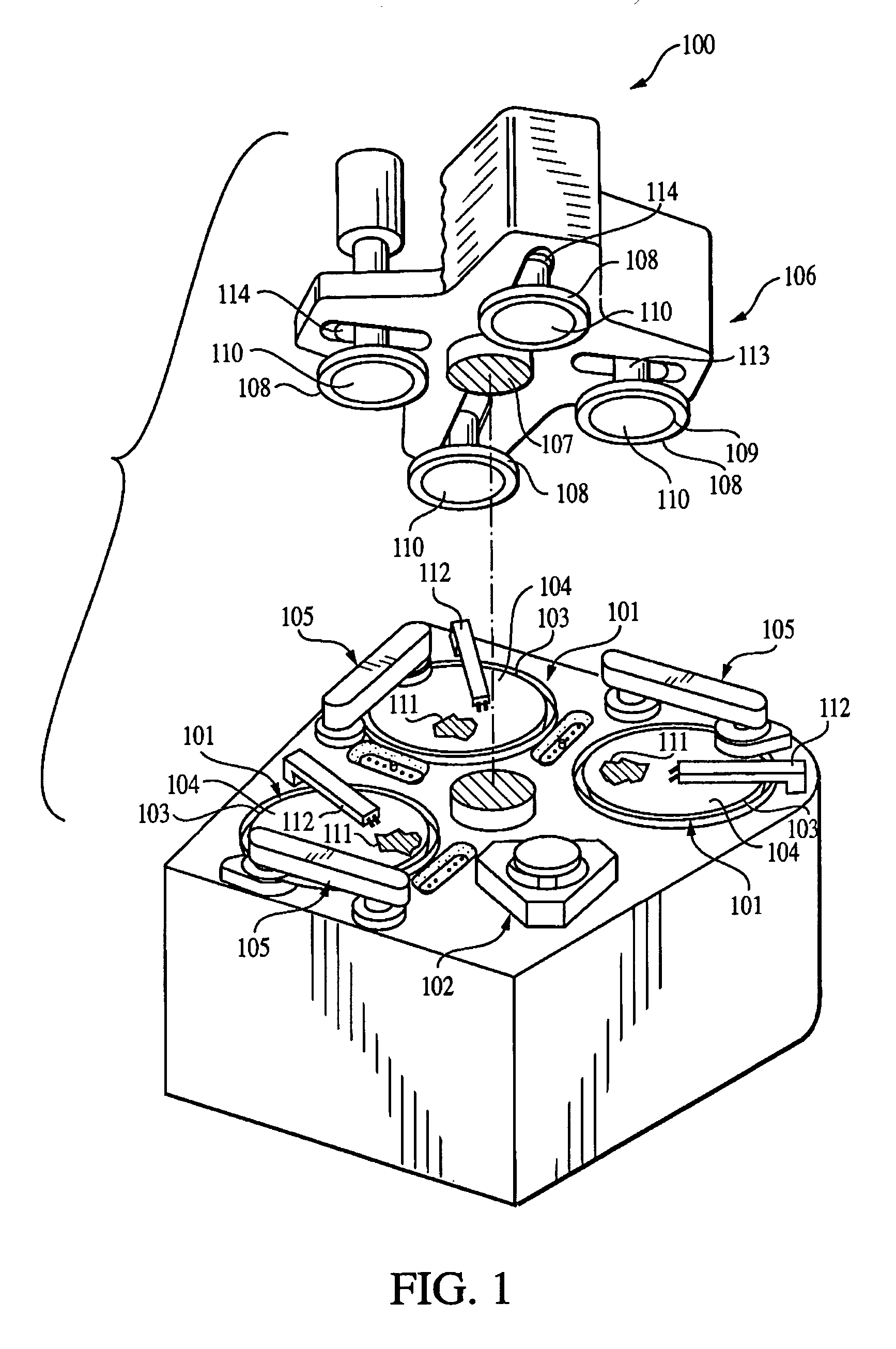
[0050]FIG. 1 shows a perspective view of a typical CMP apparatus 100 for polishing one or more substrates 110. The CMP apparatus 100 includes a series of polishing stations 101 and a transfer station 102 for loading and unloading substrates. Each polishing station includes a rotatable platen 103 on which is placed a polishing pad 104. A source of polishing fluid 111 may be provided to supply polishing fluid 112 to the polishing pad 104. Each polishing station may include an associated pad conditioning apparatus 105 to maintain the abrasive condition of the polishing pad. A rotatable multi-head carousel 106 is supported by center post 107 about which the carousel rotates. The carousel 106 includes multiple carrier heads 108 that are capable of independently rotating about its own axis. The carrier head 108 receives a substrate from and delivers a substrate to the transfer station 102. The carrier head provides a controllable load, i.e., pressure on the substrate to push is against th...


PUM

PropertyMeasurementUnit
diameteraaaaaaaaaa
thicknessaaaaaaaaaa
wafer material removal rateaaaaaaaaaa

Abstract

A method of controlling surface non-uniformity of a wafer in a polishing operation includes (a) providing a model for a wafer polishing that defines a plurality of regions on a wafer and identifies a wafer material removal rate in a polishing step of a polishing process for each of the regions, wherein the polishing process comprises a plurality of polishing steps, (b) polishing a wafer using a first polishing recipe based upon an incoming wafer thickness profile, (c) determining a wafer thickness profile for the post-polished wafer of step (b), and (d) calculating an updated polishing recipe based upon the wafer thickness profile of step (c) and the model of step (a) to maintain a target wafer thickness profile. The model can information about the tool state to improve the model quality. The method can be used to provide feedback to a plurality of platen stations.

Description

CROSS-REFERENCE TO RELATED APPLICATIONS [0001] This application is a divisional of and claims priority under 35 U.S.C. § 121 to U.S. patent application Ser. No. 09 / 943955, filed on Aug. 31, 2001, which claims priority under 35 U.S.C. § 119(e) from U.S. Provisional Patent Application No. 60 / 298,878 filed Jun. 19, 2001.FIELD OF THE INVENTION [0002] The present invention generally relates to the planarization of substrates, in particular, semiconductor wafers, and more particularly to a method and apparatus for providing feedback control of the planarization process. BACKGROUND OF THE INVENTION [0003] Chemical-mechanical polishing (CMP) is used in semiconductor fabrication processes for obtaining full planarization of a semiconductor wafer. The method involves removing material, e.g., a sacrificial layer of surface material, from the wafer (typically, silicon dioxide (SiO2)) using mechanical contact and chemical erosion. Polishing flattens out height differences, since areas of high to...

Claims


Application Information

Patent Timeline
Patent Type & Authority Applications(United States)
IPC IPC(8): G06F19/00H01L21/306B24B37/04B24B49/02B24B49/03B24B49/04B24B49/18G05B19/00G05B19/19G05B19/418H01L21/00H01L21/304H01L21/3105H01L21/66
CPCB24B37/013B24B37/042H01L2924/0002B24B49/03B24B49/04B24B49/18G05B19/00G05B19/19G05B19/41865G05B2219/32053G05B2219/32065G05B2219/45031H01L21/31053H01L21/67253H01L21/67276H01L22/20H01L2924/00Y02P90/02H01L21/304
Inventor SHANMUGASUNDRAM, ARULKUMAR P.SCHWARM, ALEXANDER T.PRABHU, GOPALAKRISHNA B.
Owner APPLIED MATERIALS INC
Why Eureka
Try Eureka