

Current limiting circuit and output circuit including the same
- Summary
- Abstract
- Description
- Claims
- Application Information
AI Technical Summary
Benefits of technology
Problems solved by technology
Method used
Image

Examples
Embodiment Construction
[0049]Various embodiments of the present invention will now be described in detail with reference to a number of drawings.
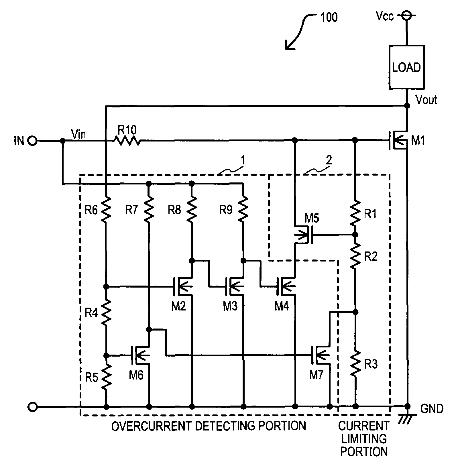
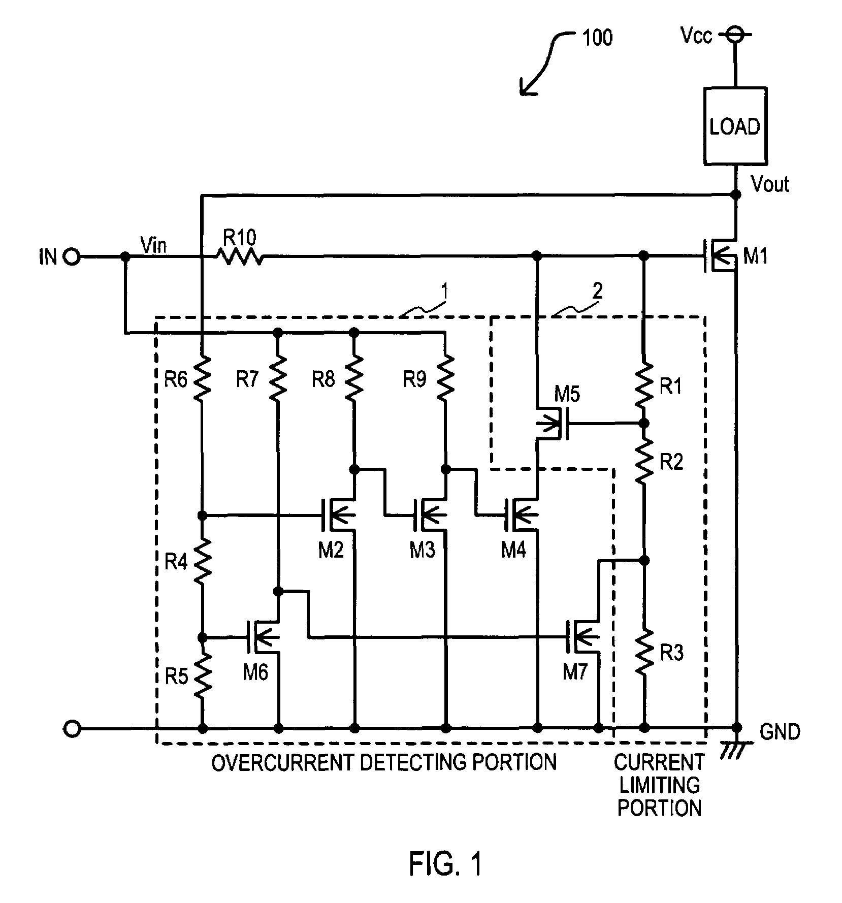
[0050]Referring now to FIG. 1, a circuit schematic diagram of an output circuit including a current limiting circuit according to an embodiment is set forth and given the general reference character 100.
[0051]Output circuit 100 may include a transistor M1, a resistor R10, a voltage detecting circuit 1, and a voltage clamping circuit 2. Transistor M1 may be an n-channel MOSFET (metal-oxide-semiconductor field effect transistor) and may be used as an output power transistor. A load LOAD may be connected between a power supply Vcc and an output terminal at a drain of transistor M1 to produce an output voltage Vout. Transistor M1 may have a source connected to a ground GND. Resistor R10 may be connected between a gate of transistor M1 and an input terminal IN.
[0052]Voltage detecting circuit 1 may be connected to the drain of transistor M1 to detect an output voltage ...
PUM
 Abstract
Description
Claims
Application Information