Flip chip interconnection pad layout

a flip chip and interconnection technology, applied in the field of flip chip interconnection pad layout, can solve the problems of high cost of multiple layer substrates, achieve the effects of reducing the number of vias, reducing the cost, and increasing the routing density of signal trace escap

Active Publication Date: 2008-05-13
STATS CHIPPAC LTD
View PDF11 Cites 8 Cited by
  • Summary
  • Abstract
  • Description
  • Claims
  • Application Information

AI Technical Summary

Benefits of technology

[0009]The pad layouts provide for higher signal trace escape routing density at the chip margin. The package substrates have fewer metal layers, so that packages constructed using the pad layout of the invention can be made at significantly lower cost. Because there are fewer metal layers, and because the number of vias is reduced (and vias can be eliminated entirely from the signal transmission path), electrical parasitics are reduced, and the package can have improved performance.

Problems solved by technology

Multiple layer substrates are expensive, and in conventional flip chip constructs the substrate alone typically accounts for more than half the package cost (about 60% in some typical instances).

Method used


Image

  • Flip chip interconnection pad layout
  • Flip chip interconnection pad layout
  • Flip chip interconnection pad layout

Examples


Embodiment Construction

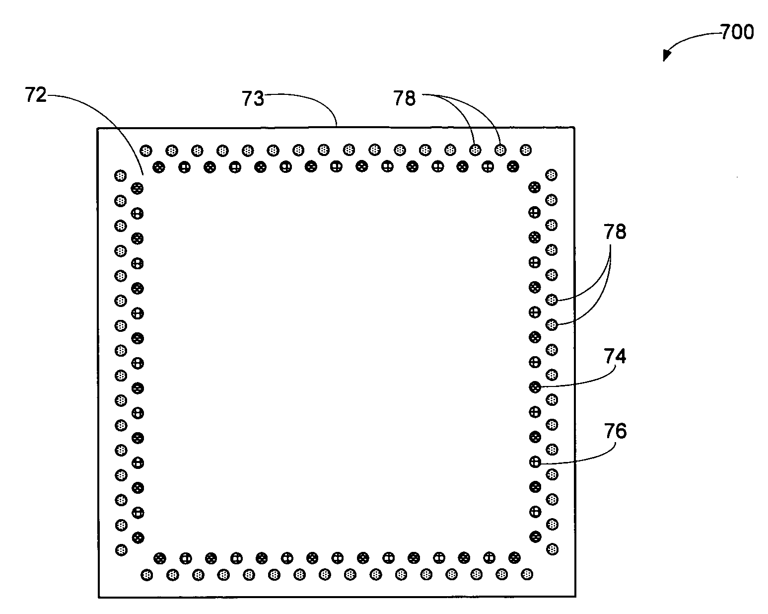
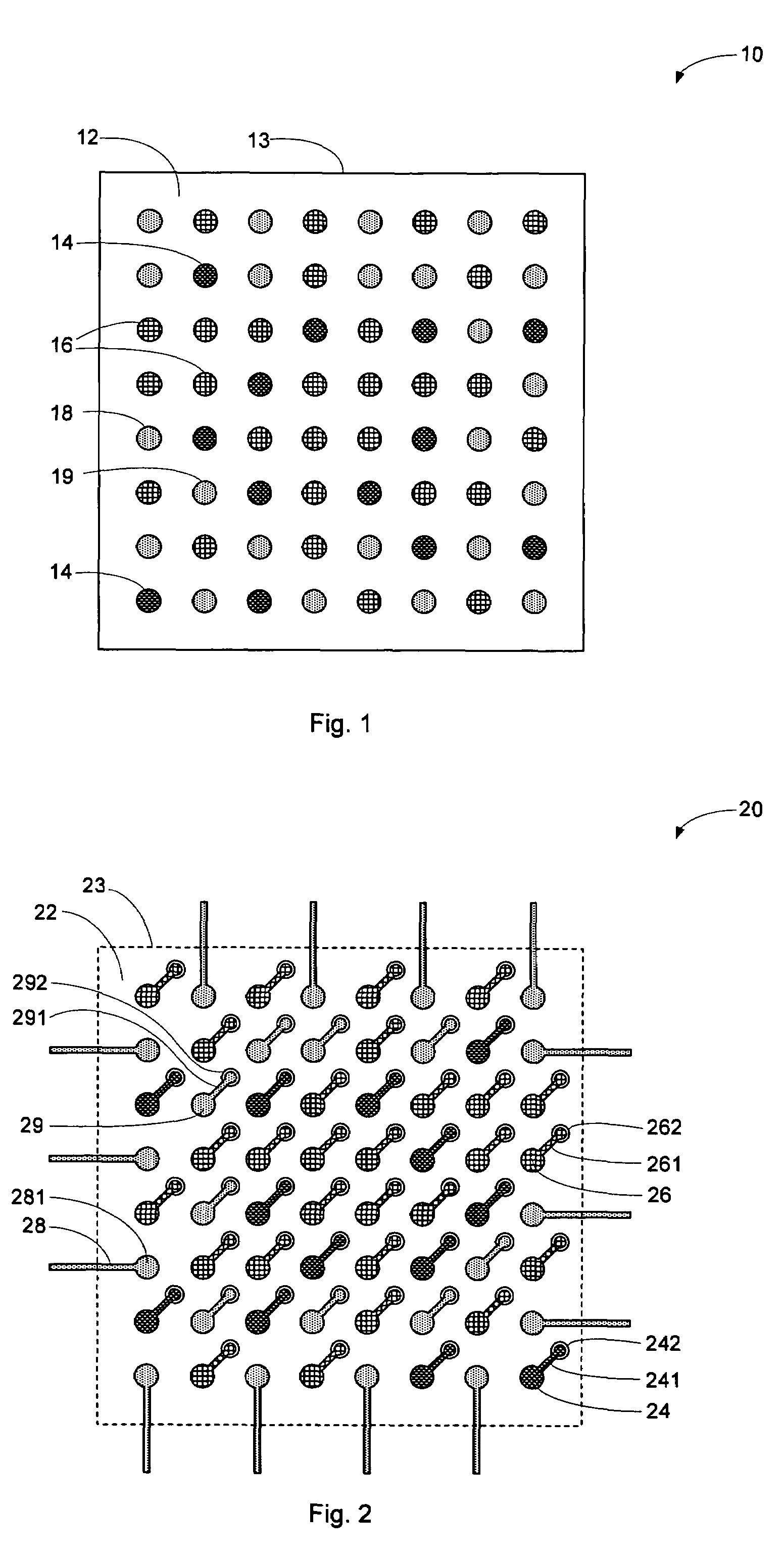
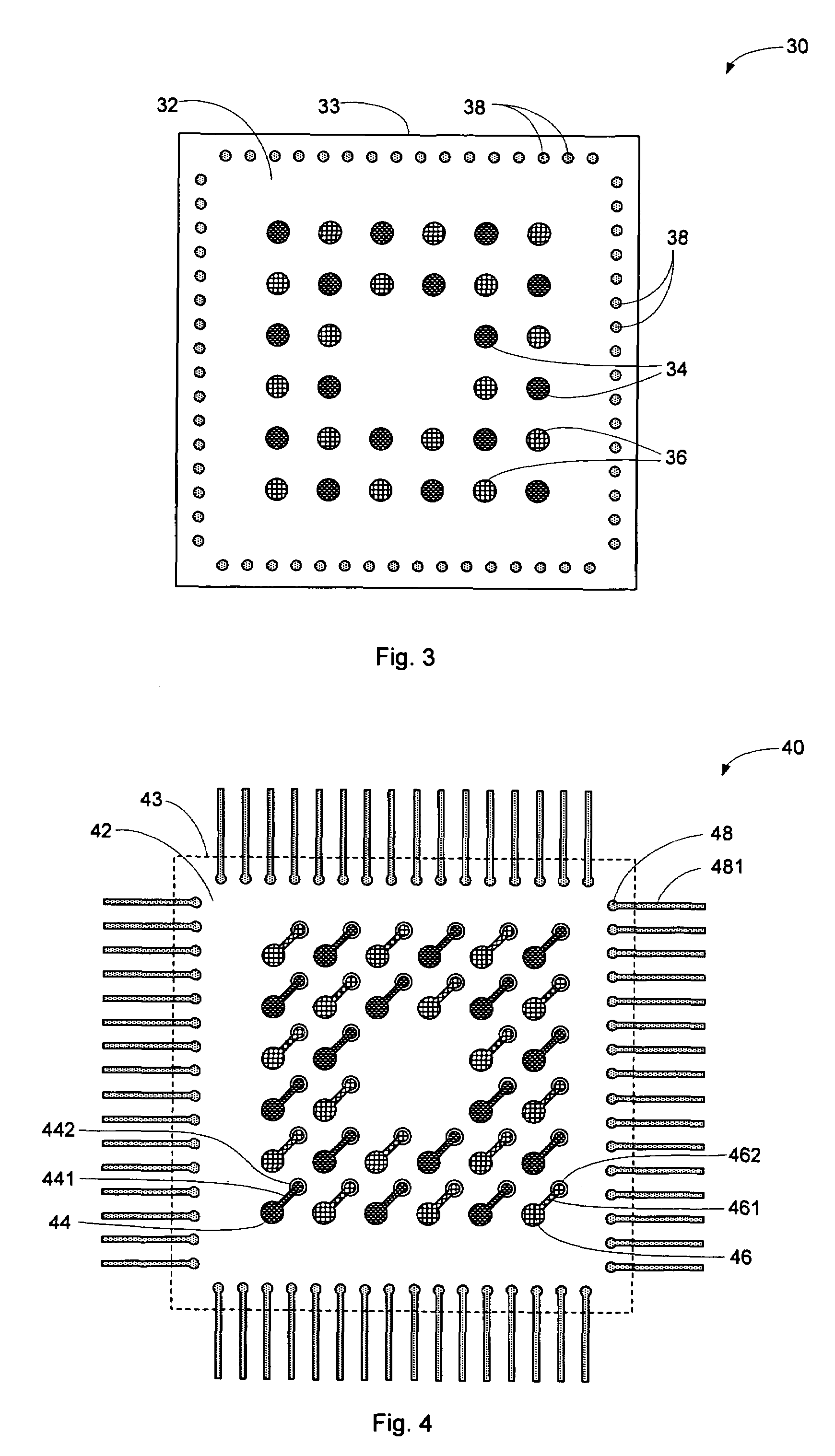
[0030]The invention will now be described in further detail by reference to the drawings, which illustrate alternative embodiments of the invention. The drawings are diagrammatic, showing features of the invention and their relation to other features and structures, and are not made to scale. For improved clarity of presentation, in the FIGS. illustrating embodiments of the invention, elements corresponding to elements shown in other drawings are not all particularly renumbered, although they are all readily identifiable in all the FIGS.

[0031]In a conventional flip chip package, the input / output pads (collectively the “signal” pads) on the die are arranged in an area array substantially covering the active face 12 of the chip, as shown by way of illustration in a plan view generally at 10 in FIG. 1. The signal pads (e.g., 18, 19), power pads (e.g., 14), and ground pads (e.g., 16) (collectively the “power / ground pads”), directed respectively to the signal, power and ground functions ...


PUM


Abstract

A flip chip interconnect pad layout has the die signal pads are arranged on the die surface near the perimeter of the die, and the die power and ground pads arranged on the die surface inboard from the signal pads; and has the signal pads on the corresponding package substrate arranged in a manner complementary to the die pad layout and the signal lines routed from the signal pads beneath the die edge away from the die footprint, and has the power and ground lines routed to vias beneath the die footprint. Also, a flip chip semiconductor package in which the flip chip interconnect pad layouts have the die signal pads situated in the marginal part of the die and the die power and ground pads arranged on the die surface inboard from the signal pads, and the corresponding package substrates have signal pads arranged in a manner complementary to the die pad layout and signal lines routed from the signal pads beneath the die edge away from the die footprint.

Description

CROSS-REFERENCE TO RELATED APPLICATIONS[0001]This application is a division of U.S. application Ser. No. 10 / 983,898, now U.S. Pat. No. 7,034,391, filed Nov. 8, 2004, titled “Flip chip interconnection pad layout”, which claims priority from U.S. Provisional Application No. 60 / 518,434, filed Nov. 8, 2003, titled “Flip chip interconnection pad layout”.BACKGROUND[0002]This invention relates to semiconductor packaging and, particularly, to interconnect pad layout for flip chip interconnect.[0003]Flip chip packages include a semiconductor die mounted onto a package substrate with the active side of the die facing the substrate. Interconnection of the circuitry in the die with circuitry in the substrate is made by way of bumps which are attached to an array of interconnect pads on the die, and bonded to a corresponding (complementary) array of interconnect pads on the substrate.[0004]The pads on the die for the signal, power and ground functions of the die are conventionally distributed th...

Claims


Application Information

Patent Timeline
Patent Type & Authority Patents(United States)
IPC IPC(8): H01L21/82H01L23/28H01L29/40H05K7/00H01L21/60H01L23/498H01L23/50
CPCH01L23/49838H01L23/50H01L24/81H01L2224/16225H01L2924/15311H01L2924/3011H01L2924/3025H01L2224/81801H01L2224/05568H01L2224/05573
Inventor PENDSE, RAJENDRA D.
Owner STATS CHIPPAC LTD
Why Eureka
Try Eureka