

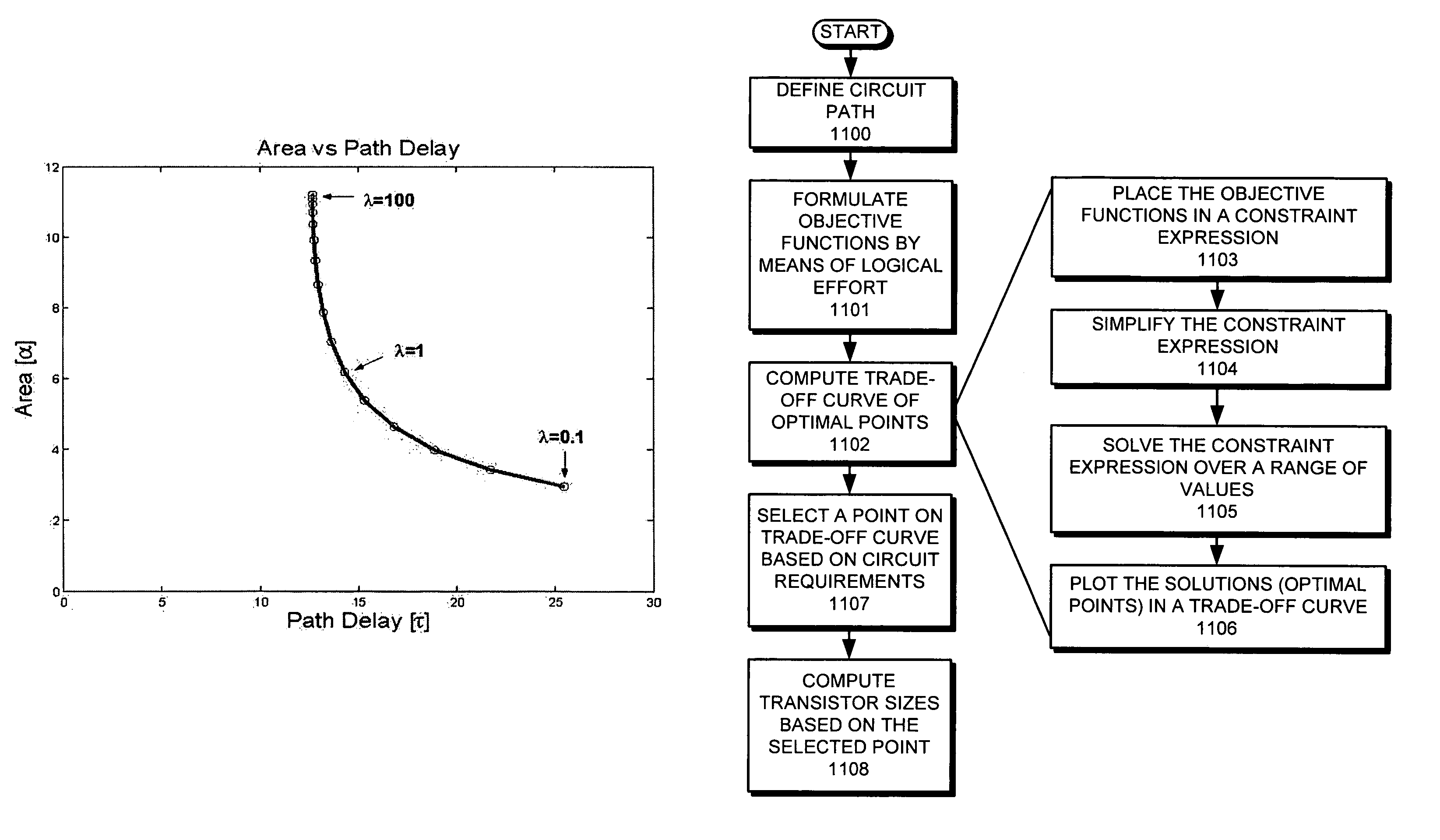
Performing a constrained optimization to determine circuit parameters
a technology of constrained optimization and circuit parameters, applied in multi-objective optimization, cad techniques, instruments, etc., can solve the problems of prohibitive run-times, limiting the effectiveness of many applications of interest, and outright failure of some applications
- Summary
- Abstract
- Description
- Claims
- Application Information
AI Technical Summary
Benefits of technology
Problems solved by technology
Method used
Image

Examples
an example
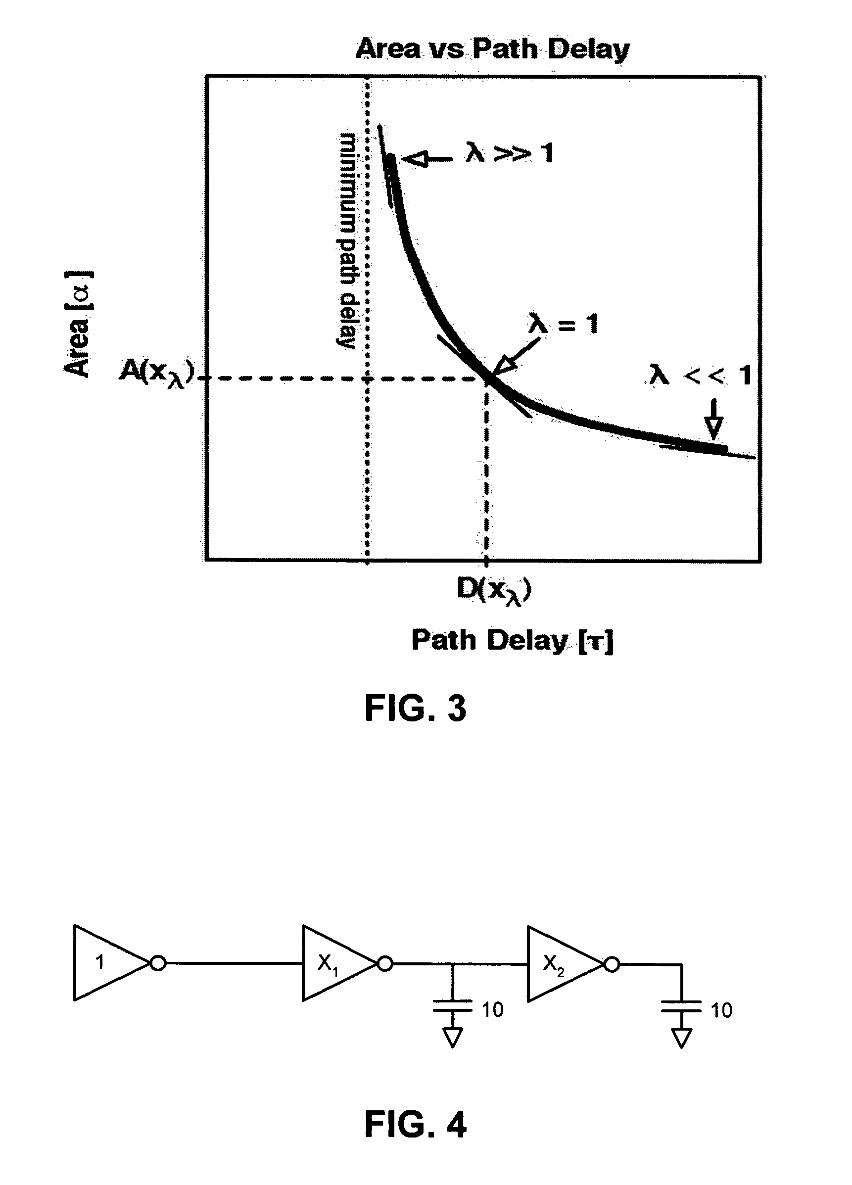
[0083]FIG. 4 illustrates a string of three inverters with one side load and one final load in accordance with an embodiment of the present invention. Both loads associated with the circuit are 10 and drive strength x0=1. The functions D(x) and A(x) are as follows:
D(x)=(1+x1 / 1)+(1+10 / x1+x2 / x1)+(1+10 / x2)A(x)=1+x1+x2.
[0084]Let us compute the area versus delay function for this example. For each λ we have to find xλ satisfying ∇A(x)=−λ∇D(x) where ∇A(x)=[1, 1]. Because all gates are inverters, we have gi=1 and tgi=1 for i=1, 2. The update functions for x1 and x2 are:
[0085]x1=10+x2(1 / λ)+1x2=10(1 / λ)+1 / x1.
[0086]Let us first calculate the minimum path delay. For this purpose we choose λ=∞. The update functions now simplify to:
x1=√{square root over (10+x2)}
x2=√{square root over (10*x1)}
[0087]Table 1 provides the successive values for (x1, x2) during the execution of the coordinate-wise descent algorithm. After only six steps, or three vector values, the algorithm yields values for (x1, x2) ...
second example
A Second Example
[0092]In this example we consider a network with cycles. We find the area versus delay function and the energy versus delay function for one segment of this chain of C-elements. FIG. 7 illustrates a chain of C-elements connected in a ring and FIG. 8 illustrates a segment from a chain of C-elements in accordance with an embodiment of the present invention.
[0093]When performing a constrained optimization on the circuit of FIG. 7, if we need to consider every gate in this chain of C-elements, the task is unmanageable. For our analysis purposes, however, we only consider the segment of FIG. 8, where terminals labeled A connect to each other and terminals labeled B connect to each other. Note that we labeled each input and output of a gate with the logical effort or parasitic delay of that terminal.
[0094]The delay function D(x) for this circuit is the cycle time of the cycle containing an inverter and two C-elements. The delay function is
D(x)=(1+2*x2 / x1)+2*(2+(CL+x1+2*x2)...
PUM
 Abstract
Description
Claims
Application Information