Wiring board manufacturing method

a manufacturing method and wire technology, applied in the direction of printed element electric connection formation, semiconductor/solid-state device details, printed circuit non-printed electric components association, etc., can solve the problem of inability to high-density wire density, achieve high density, increase rigidity of the core substrate, and high wiring density

Inactive Publication Date: 2008-05-27
FUJITSU LTD
View PDF6 Cites 6 Cited by
  • Summary
  • Abstract
  • Description
  • Claims
  • Application Information

AI Technical Summary

Benefits of technology

[0011]Since the build-up layer and the core substrate are separately formed, the build-up layer is not limited by size, etc. of through-holes bored in the core substrate so that the wiring patterns can be formed with high density. Rigidity of the core substrate can be increased by selecting a material and a producing process. By effectively taking advantageous characteristics of the build-up layer and the core substrate, the wiring board having high wiring density, low thermal expansion coefficient and high rigidity can be produced.
[0012]In another method of manufacturing a wiring board, in which build-up layers are formed on both sides of a core substrate, metal films, whose thermal expansion coefficients are lower than that of copper, are included in the build-up layers and located at positions not interfering with wiring patterns. With this method, the metal films having low thermal expansion coefficients are included in the build-up layers, so that a thermal expansion coefficient of the wiring board can be made lower and thermal stress between the wiring board and semiconductor chips can be restrained.

Problems solved by technology

However, if the core substrate is made thin, a special conveying mechanism is required, and rigidity of the wiring board is lowered so that the wiring board will be shrunk or waved due to stress caused in the steps of forming insulating layers, wiring patterns, etc. and wiring density cannot be high.

Method used


Image

  • Wiring board manufacturing method
  • Wiring board manufacturing method
  • Wiring board manufacturing method

Examples


embodiment 1

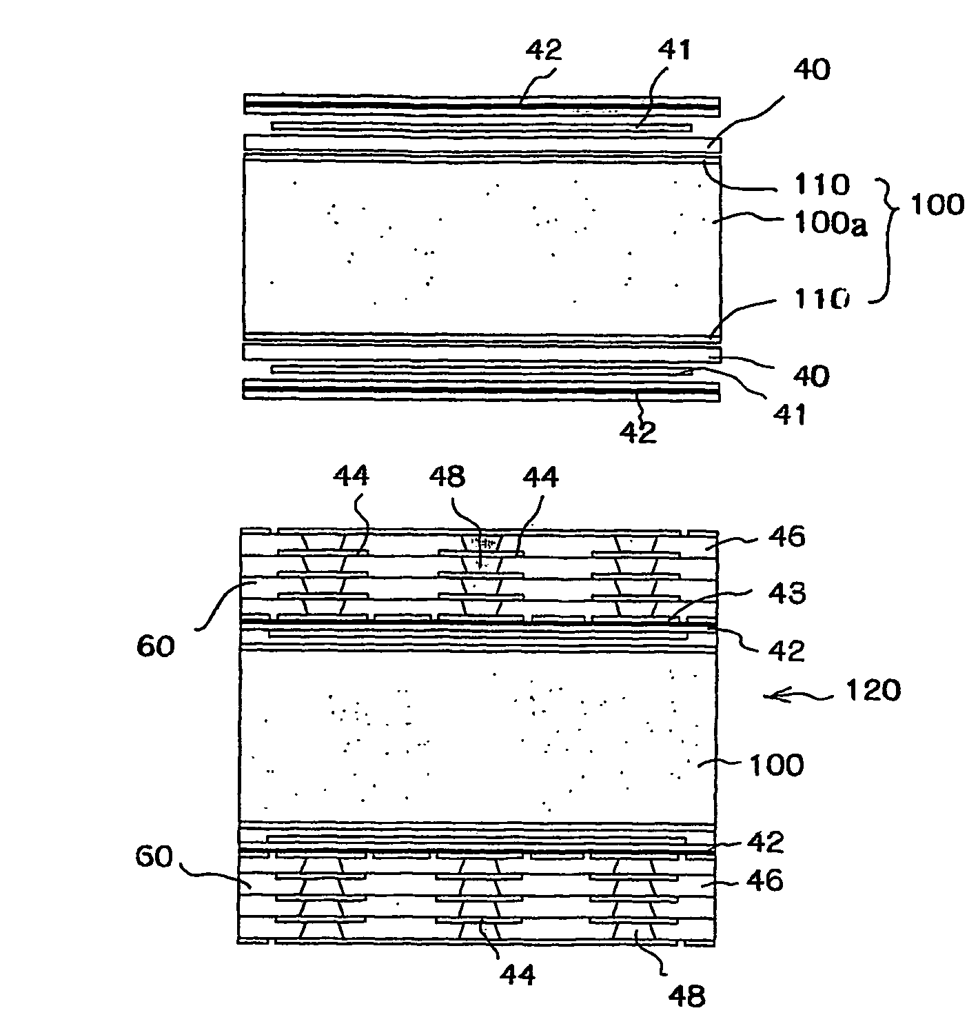
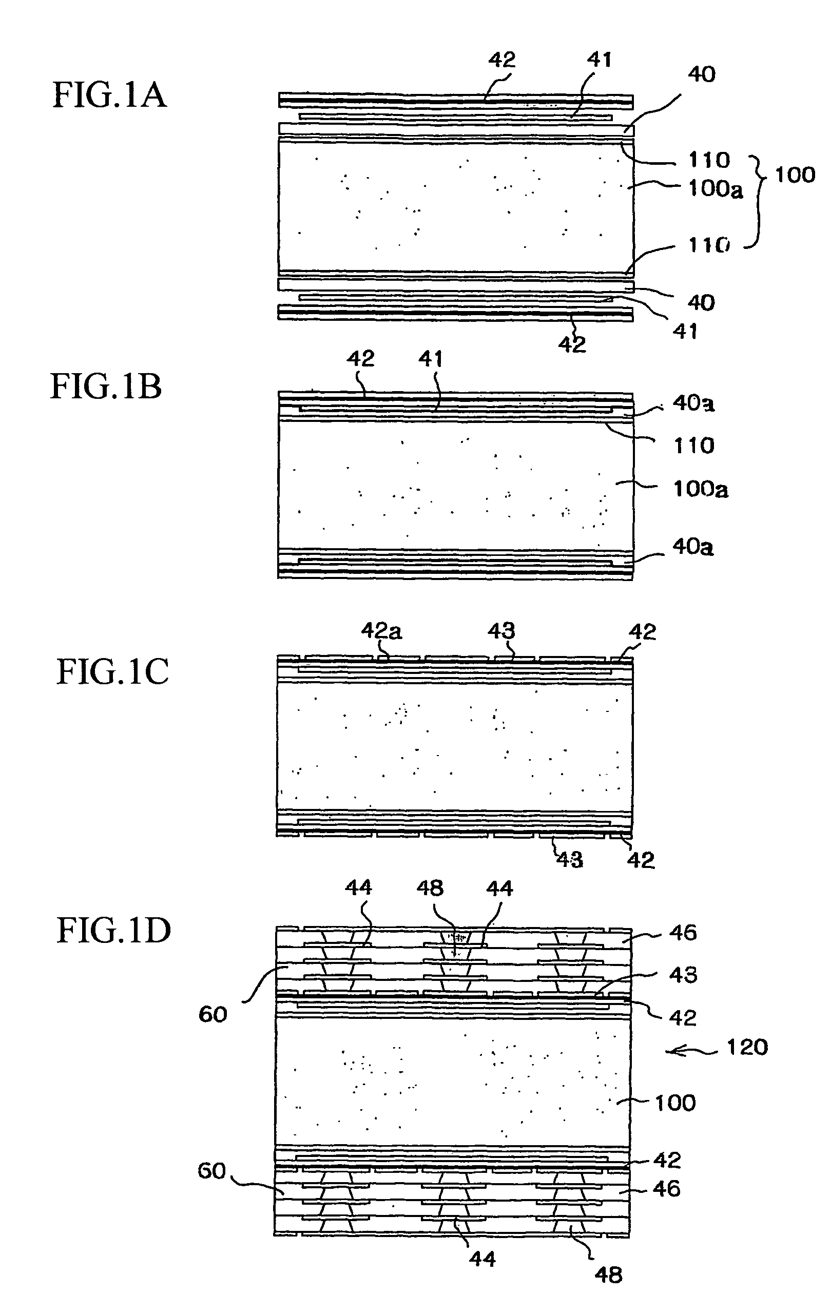
[0026]FIGS. 1-4 shows the wiring board manufacturing method of the present invention. FIG. 1A shows a characteristic step of the method, wherein a first metal layer 41 and a second metal layer 42 are respectively adhered on both side faces of a support 100 by adhesive films 40.

[0027]The support 100 is used as a base, on which wiring patterns are formed by the build-up process, and made of a material having enough rigidity so as not to deform while forming build-up layers. In the present embodiment, a base member 100a of the support 100 is an epoxy resin plate, which includes glass cloth and whose thickness is 0.3-0.4 mm, and both side faces of the support 100 is covered with copper films 11, whose thickness are 9 μm. The support 100 is a large plate, in which a plurality of wiring boards can be formed.

[0028]One of the adhesive films 40 adheres and fixes the first metal layer 41 on the support 100; the other film adheres an outer edge part of the second metal layer 42 on the support ...

embodiment 2

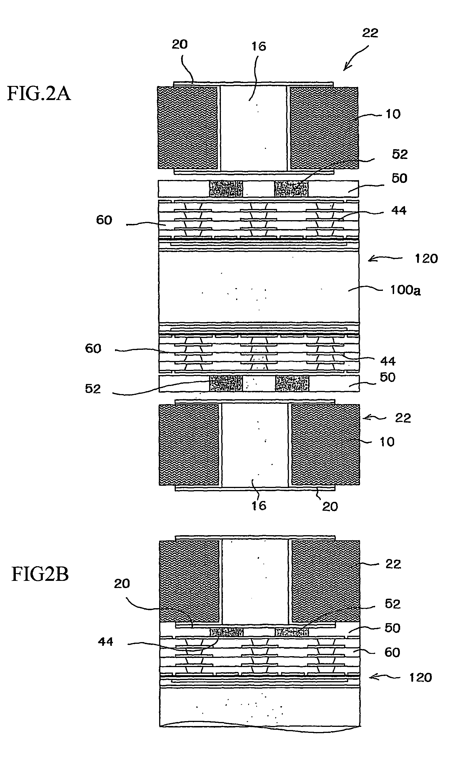
[0043]In the present embodiment, the core substrate 10 is produced by the conventional method shown in FIG. 12, then a metal film, which has a low thermal expansion coefficient, is included in build-up layer, so that a thermal expansion coefficient of the wiring board can be approximated to that of a semiconductor chip.

[0044]In FIG. 6A, build-up layers 60 are formed on both side faces of a core substrate 22. Symbols 44 stand for wiring patterns; a symbol 46 stands for an insulating layer; and a symbol 48 stand for a via.

[0045]In FIG. 6B, an adhesive metal film 84, which is constituted by a metal film 80, e.g., metal alloy 42, whose thermal expansion coefficient is lower than that of copper, and an adhesive layer 82, and holes 84a are formed therein by proper means, e.g., drill, laser, etching. By forming the hole 84a, the adhesive metal film 84 does not interfere with the wiring the build-up layers 60 when the adhesive metal film is adhered onto the build-up layers 60.

[0046]In FIG. ...


PUM

PropertyMeasurementUnit
thicknessaaaaaaaaaa
thicknessaaaaaaaaaa
insulatingaaaaaaaaaa

Abstract

The present invention relates to a method of manufacturing a wiring board comprising: a build-up layer, in which wiring patterns are piled with insulating layers; and a core substrate, which is separately formed from the build-up layer, the method comprising the steps of: separably forming the build-up layer on a plate-shaped support; electrically connecting the core substrate to the wiring patterns of the build-up layer on the support; and removing the support from the build-up layer so as to form the wiring board, in which the build-up layer is connected to the core substrate. By separably forming the build-up layer and the core substrate, the wiring board effectively exhibiting characteristics thereof can be produced.

Description

[0001]This application is a continuation of international application PCT / JP / 2003 / 006492, filed on May 23, 2003.FIELD OF TECHNOLOGY[0002]The present invention relates to a wiring board manufacturing method, more precisely relates to a method of manufacturing a wiring board having high wiring density, low thermal expansion coefficient and high rigidity.BACKGROUND OF TECHNOLOGY[0003]A conventional wiring board manufacturing method, in which wiring patterns are formed on both sides of a core substrate by a build-up process, is shown in FIGS. 12 and 13.[0004]A process of producing the core substrate 22, in which the wiring patterns are formed on the both sides, is shown in FIG. 12. A base board 10, in which copper films are adhered on both sides, is shown in FIG. 12A. The base board 10 is formed by adhering copper films 11 on the both side faces of a board member 10a, which is made of epoxy resin including glass cloth. In FIG. 12B, through-holes 12 are bored in the base board 10 by a dr...

Claims


Application Information

Patent Timeline
Patent Type & Authority Patents(United States)
IPC IPC(8): H05K3/36H01L21/48H01L21/68H05K1/02H05K1/11H05K1/18H05K3/20H05K3/40H05K3/46
CPCH01L21/4857H01L21/6835H01L23/49822H01L23/49827H05K1/0271H05K1/113H05K3/4602H05K3/4682H01L21/486Y10T29/49117H01L23/142H01L2224/16H01L2924/01004H01L2924/01078H01L2924/01079H01L2924/19041H01L2924/19106H05K1/0231H05K1/183H05K3/20H05K3/4069H05K3/4614H05K3/4644H05K3/4652H05K3/4697H05K2201/0347H05K2201/0355H05K2201/0391H05K2201/068H05K2201/0959H05K2201/096H05K2201/09781H05K2201/10378H05K2201/10545H05K2201/10674H05K2203/0156H05K2203/016H05K2203/061H05K2203/085H05K2203/1536H01L2224/16235Y10T29/49169Y10T29/4913Y10T29/49155Y10T29/49156Y10T29/49128Y10T29/49126H01L2924/00014H01L2924/00011H01L2224/0401
Inventor SHUTO, TAKASHITAKANO, KENJIILDA, KENJIABE, KENICHIROARAI, KEIJISEYAMA, KIYOTAKA
Owner FUJITSU LTD
Why Eureka
Try Eureka