Display device and electronic device

Active Publication Date: 2009-07-02
JOLED INC
View PDF17 Cites 4 Cited by
  • Summary
  • Abstract
  • Description
  • Claims
  • Application Information

AI Technical Summary

Benefits of technology

[0013]According to an embodiment of the present invention, an active matrix type display device is configured such that the output of one of a pair of vertical driving circuits that determine the driving of pixels is alternately input to pixels adjacent to each other in an upper row and a lower row. Thereby, a signal line extending in a vertical direction from each output stage of a horizontal driving circuit can be shared between pixels adjacent to each other in a left column and a right column. By sharing one signal line between pixels in two columns, the total number of signal lines can be halved. It is possible to lower the wiring density of signa

Problems solved by technology

Thereby, the wiring density of signal lines in the pixel array section has become higher, which invites an increase in the percentage of defectives such as short-circuit defects or the like.
With the increase in the number of output stages including a switch element, the horizontal driving circuit has become compli

Method used


Image

  • Display device and electronic device
  • Display device and electronic device
  • Display device and electronic device

Examples


Embodiment Construction

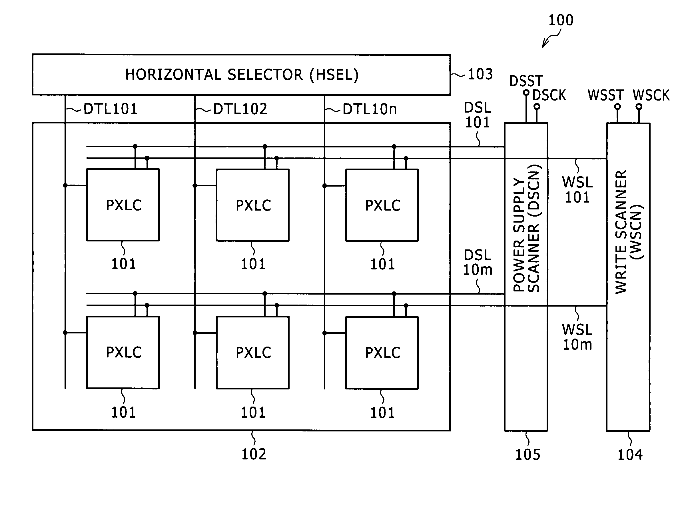
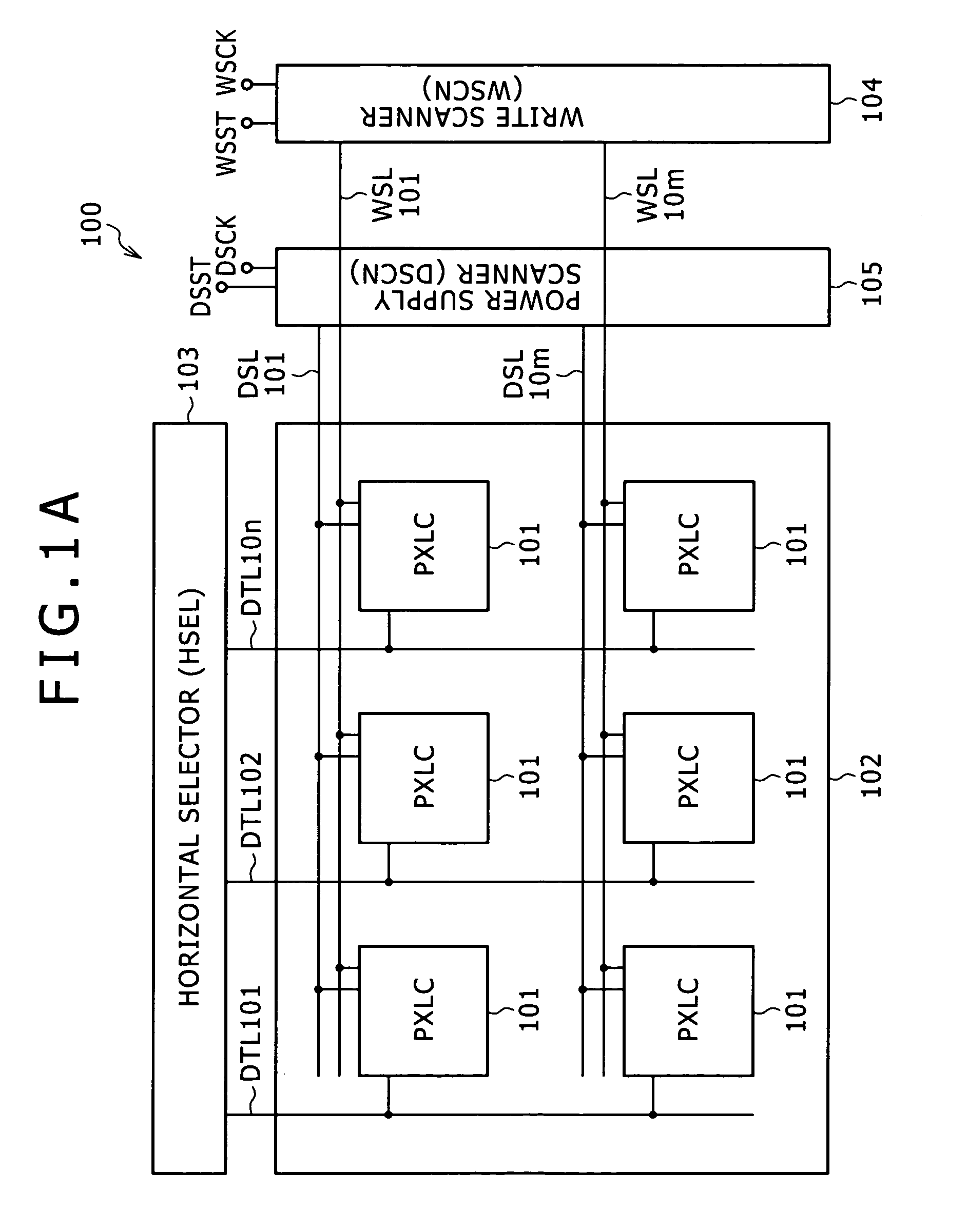
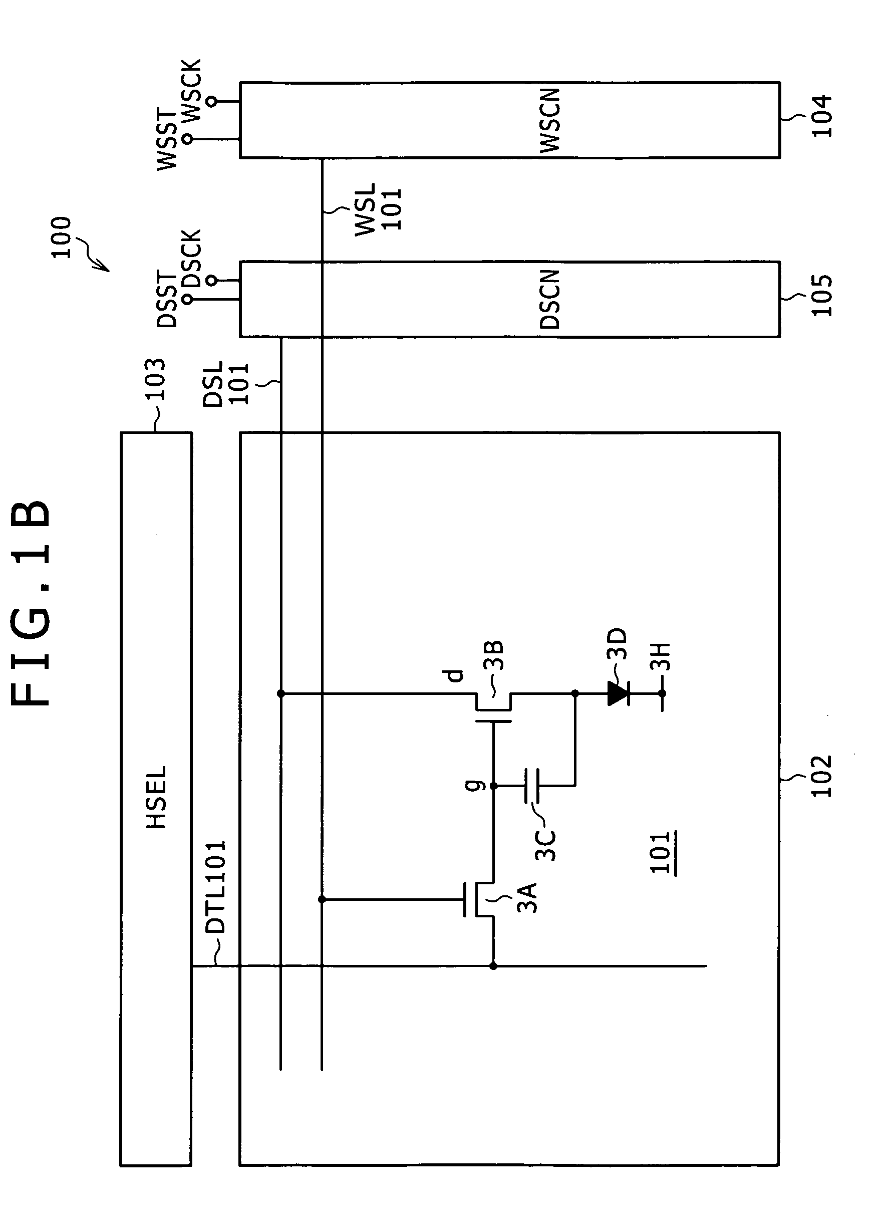
[0058]Preferred embodiment of the present invention will hereinafter be described in detail with reference to the drawings. First, in order to clarify the background of the present invention and facilitate understanding, an ordinary configuration of an active matrix type display device will be described as a reference example. FIG. 1A is a block diagram showing a general configuration of the display device according to the reference example. As shown in FIG. 1A, the display device 100 includes a pixel array section 102 and a driving section (103, 104, and 105) for driving the pixel array section 102. The pixel array section 102 includes scanning lines WSL101 to WSL10m in the form of rows, signal lines DTL101 to DTL10n in the form of columns, pixels (PIX) 101 in the form of a matrix which pixels are arranged at parts where the scanning lines WSL101 to WSL10m intersect the signal lines DTL101 to DTL10n , and feeding lines DSL101 to DSL10m arranged so as to correspond to the respective...


PUM


Abstract

The present invention provides a display device includes: a pixel array section including a set of pixels arranged in a form of a matrix; and a driving section for driving the pixel array section.

Description

CROSS REFERENCES TO RELATED APPLICATIONS[0001]The present invention contains subject matter related to Japanese Patent Application JP 2007-336792, filed in the Japan Patent Office on Dec. 27, 2007, the entire contents of which being incorporated herein by reference.BACKGROUND OF THE INVENTION[0002]1. Field of the Invention[0003]The present invention relates to an active matrix type display device using a light emitting element in a pixel, and an electronic device incorporating such a display device.[0004]2. Description of the Related Art[0005]Development of flat-panel emissive display devices using an organic EL (electro luminescence) device as a light emitting element has recently been actively underway. The organic EL device uses a phenomenon in which an organic thin film emits light when an electric field is applied to the organic thin film. The organic EL device is driven with an applied voltage of 10 V or lower, and thus consumes low power. In addition, the organic EL device is...

Claims


Application Information

Patent Timeline
IPC IPC(8): G09G3/30
CPCG09G3/3233G09G3/3266G09G3/3291G09G2320/043G09G2300/0842G09G2300/0866G09G2300/0408H01L2924/13069
Inventor TANIKAME, TAKAO
Owner JOLED INC
Why Eureka
Try Eureka