System and method for cleaning semicondutor fabrication equipment parts

a technology for fabrication equipment and parts, applied in the direction of cleaning using liquids, inorganic non-surface active detergent compositions, instruments, etc., can solve the problems of contaminated equipment used in the semiconductor processing process, unusable, missed transfers, etc., to reduce cleaning defects, enhance cleaning process, and increase accuracy

Inactive Publication Date: 2005-03-03
TAN SAMANTHA
View PDF7 Cites 51 Cited by
  • Summary
  • Abstract
  • Description
  • Claims
  • Application Information

AI Technical Summary

Benefits of technology

[0010] Advantageously, one embodiment of the present invention reduces the cleaning defects by use of repeated testing of the impurity levels after each pass through the cleaning process. Moreover, by knowing the characteristics of a clean part through testing, the process of the present invention can achieve particular impurity level goals with increased accuracy, and the part can be certified to meet an actual specification based on either the need for cleanliness in the semiconductor process, or based on statistically significant test data. Finally, the process may be continuously optimized to further enhance the cleaning process by direct testing of the cleanliness of the part, by correlating to number of “added” particles and RF hours that the parts can be used before particles increase to unacceptable limits, and ultimately by correlating to improved wafer yield.
[0012] Advantageously, dilute chemistries can be used in preferred embodiments of the present invention. This makes the cleaning process less expensive. Used chemicals are also easier to dispose of because the percentage of acids is much lower which also in turn makes it less hazardous. Additionally, there is less damage to the product. The present invention further includes methodologies to determine optimal chemistries which are effective, yet dilute.

Problems solved by technology

Furthermore, after many wafers have been processed, the equipment used in the semiconductor processing process becomes contaminated, and therefore unusable.
This results in non-uniform etching across the wafer as well as missed transfers due to a wafer sticking to polymer buildup on the electrode.
Non-uniformity exceeding seven percent is beyond some specified limits, in turn affecting side wall profile variance across the wafer.
Since, there are many variations to the wafer processes, the polymer and contamination levels of a used chamber part is different, therefore, merely following one cleaning recipe does not always result in the part being cleaned.
In addition, after following the cleaning recipe, a conventional cleaning house generally will not test the parts to ensure its cleanliness.
In general, a conventional cleaning house has no idea as to the effectiveness of the cleaning process provided to them in the recipe.
The result of following cleaning recipes in this manner, is that many semiconductor parts are returned to the semiconductor manufacturing plant still contaminated with unacceptable levels of impurities.
This results in contamination that may be transferred onto a wafer typically in the form of high particle counts, or in inoperable equipment that must again be disassembled for re-cleaning, thus further increasing the down time for the equipment.
Chamber parts manufactured from these base materials are very expensive and are selected because of they are non-contaminating with respect to metallics, organics and particles.
Unfortunately, such high concentration solutions suffer from a number of drawbacks.
For one, they can damage the surface of part being cleaned by scoring, etching, pitting, etc.
Further, these high concentration solutions tend to be expensive, hazardous, and difficult to dispose of.

Method used


Image

  • System and method for cleaning semicondutor fabrication equipment parts
  • System and method for cleaning semicondutor fabrication equipment parts
  • System and method for cleaning semicondutor fabrication equipment parts

Examples


Embodiment Construction

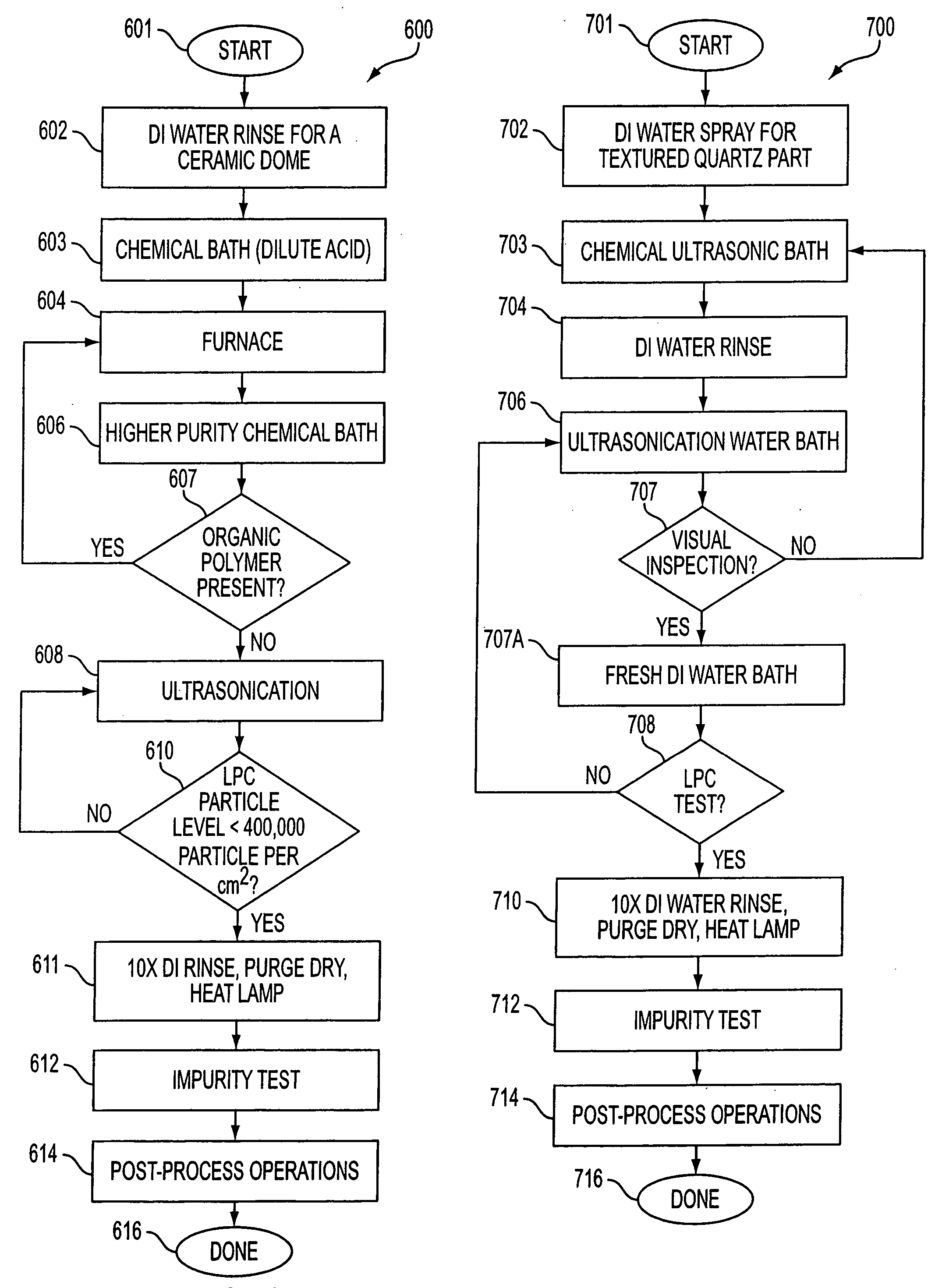
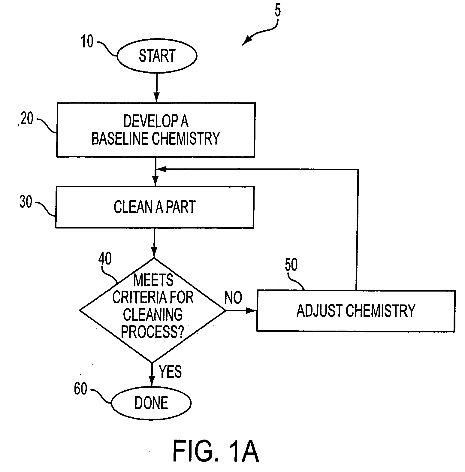
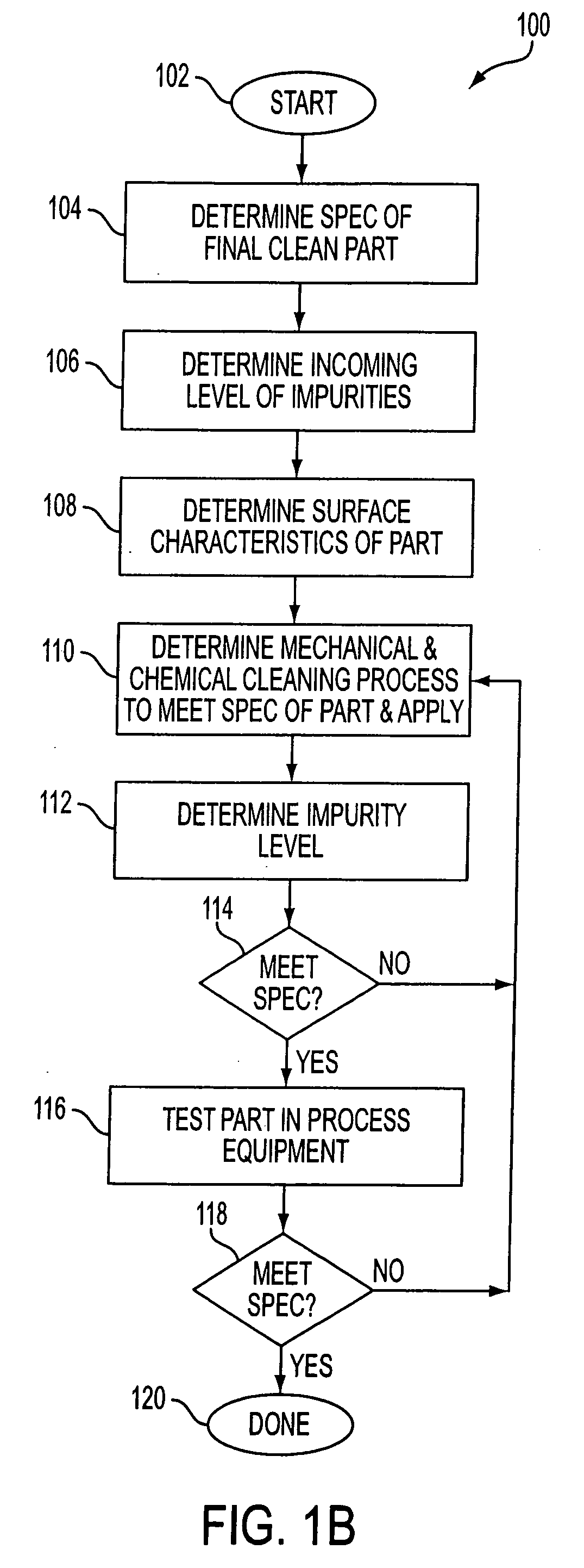
[0024] An invention is described herein for cleaning semiconductor equipment parts (such as CVD and etch chamber parts) that achieve increased effectiveness in impurity removal. In the following description, numerous specific details are set forth in order to provide a thorough understanding of the present invention. It will be apparent, however, to those skilled in the art, that the present invention may be practiced without some or all of these specific details. In other instances, well known process steps have not been described in detail in order not to unnecessarily obscure the present invention. In particular, this includes most of the analytical testing methods used to measure or confirm impurity levels.

[0025] In accordance with one aspect of the present invention, the aforementioned metallic impurity removal is substantially enhanced by the use of a new chemical formula in the various cleaning processes. This cleaning formula is particularly novel as applied to the cleaning...


PUM

PropertyMeasurementUnit
diameteraaaaaaaaaa
temperatureaaaaaaaaaa

Abstract

A process for cleaning semiconductor fabrication equipment parts includes determining a definition for a clean part including multiple maximum acceptable impurity levels; determining an initial multiple impurity levels of a part prior to its cleaning; determining a cleaning process to apply to the part; applying the cleaning process to the part, wherein the cleaning process creates reduced multiple impurity levels for the part below that of the initial multiple impurity levels; determining the reduced multiple impurity levels; comparing the reduced multiple impurity levels against the multiple maximum acceptable impurities levels of the definition; and repeating the application of the cleaning process to the part if the reduced multiple impurity levels do not meet the definition of a clean part. A dilute aqueous cleaning solution for cleaning parts includes 0.5-1.5% wt. HF; 0.1-0.5% wt. HNO3; and 1-10% wt H2O2. A method for reducing sub-surface damage to a part includes determining how deep is the sub-surface damage beneath a surface of a part; chemically etching said surface of said part; and stopping said chemical etching of said surface at about said depth of said sub-surface damage.

Description

CROSS REFERENCE TO RELATED APPLICATIONS [0001] This application claims the benefit of provisional application U.S. Ser. No. 60 / 224 / 582 (Atty. Docket No. 60081-300500), filed on Aug. 11, 2001, entitled “System and Method for Cleaning Semiconductor Fabrication Equipment Parts”, incorporated herein by reference.BACKGROUND OF THE INVENTION [0002] The commercial fabrication of semiconductor chips is performed on silicon wafer substrates, which are typically four to twelve inches in diameter. There are often more than 100 processing steps in the fabrication of semiconductor chips including oxidation, diffusion, ion implantation, deposition of conductors and insulators, photolithography, and etching. Various conducting and insulating layers are deposited uniformly over the wafer to a thickness of a few microns. [0003] In critical applications, certain new parts of semiconductor processing equipment need to be cleaned prior to installation and use in order to remove residual contamination f...

Claims


Application Information

Patent Timeline
Patent Type & Authority Applications(United States)
IPC IPC(8): B08B3/00B08B3/08C11D3/39C11D7/08C11D11/00C23C16/44H01L21/00
CPCB08B3/00B08B3/08B08B3/12C11D3/3947C11D7/08Y10T436/12C23C16/4407H01L21/67253Y10S134/902B44C1/227C11D11/0047B44C1/22
Inventor TAN, SAMANTHA
Owner TAN SAMANTHA
Why Eureka
Try Eureka