Chip package and bump connecting structure thereof

a technology of bump connecting structure and chip package, which is applied in the direction of printed circuit aspects, sustainable manufacturing/processing, final product manufacturing, etc., can solve the problems of reducing the reliability of the flip chip packag

Active Publication Date: 2008-06-03
VIA TECH INC
View PDF8 Cites 98 Cited by
  • Summary
  • Abstract
  • Description
  • Claims
  • Application Information

AI Technical Summary

Problems solved by technology

However, after the aforementioned flip chip package 100 has been used for a long time, cracks may appear on the side of the solder bumps 130 (especially solder bumps of lead-free solder) close to the chip pads 114, that results in the decrease of the reliability of the flip chip package 100.
In addition, cracks may also appear on the side of the solder bumps 130 (especially solder bumps of lead-free solder) close to the bump pads 124, that results in the decrease of the reliability of the flip chip package 100.

Method used


Image

  • Chip package and bump connecting structure thereof
  • Chip package and bump connecting structure thereof
  • Chip package and bump connecting structure thereof

Examples


Embodiment Construction

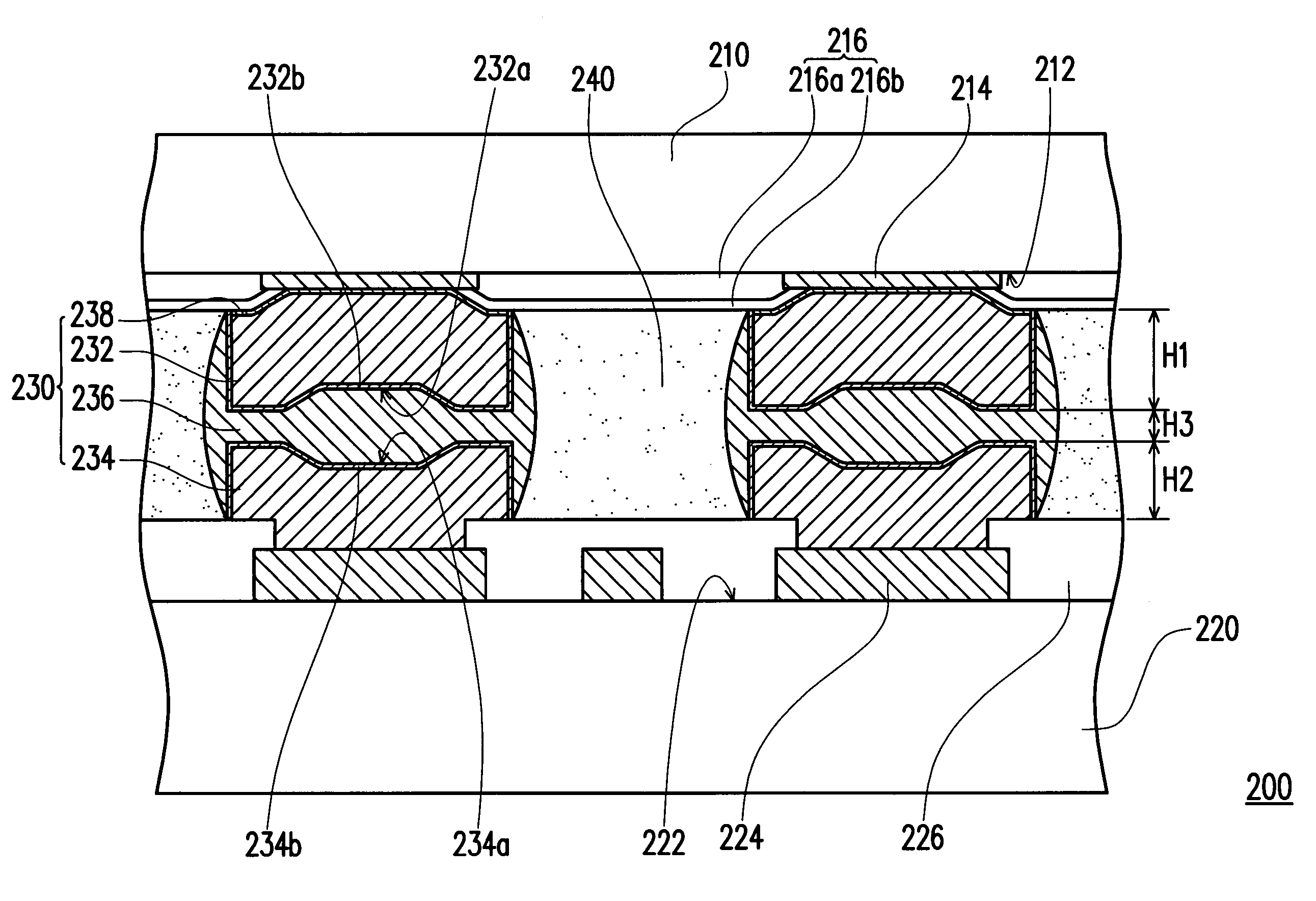
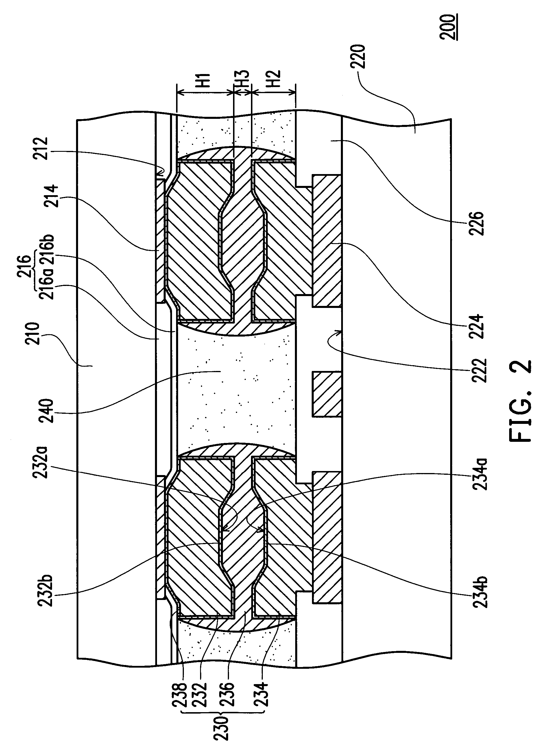
[0020]Referring to FIG. 2, which is a cross-section view of a chip package according to an embodiment of the present invention. The chip package 200 of the present embodiment includes a chip 210, a carrier 220, and a plurality of bump connecting structures 230, wherein the chip 210 is electrically connected to the carrier 220 through the bump connecting structures 230. In the present embodiment, the chip package 200 is, for example, a flip chip package, and the carrier 200 is, for example, a package substrate. The chip 210 has an active surface 212, a plurality of chip pads 214 disposed on the active surface 212, and a passivation layer 216 disposed on the active surface 212 and exposing the chip pads 214. In the present embodiment, the passivation layer 216 includes a sub-passivation layer 216a, and a stress buffer layer 216b disposed on the sub-passivation layer 216a. The material of the stress buffer layer 216b is, for example, BenzoCycloButene (BCB) or polyimide (PI). In additio...


PUM


Abstract

A chip package includes a chip, a carrier, and at least a bump connecting structure for connecting the chip to the carrier. The bump connecting structure includes a first metal bump disposed on a chip pad of the chip and has a first height relative to a passivation layer of the chip, a second metal bump disposed on a carrier pad of the carrier and has a second height relative to a solder mask layer of the carrier, and a middle metal part disposed between the first and the second metal bumps. The sum of the minimum distance between the first and the second metal bumps, the first height of the first metal bump, and the second height of the second metal bump is less than 60 micrometers. The melting point of the middle metal part is lower than that of the first and the second metal bumps.

Description

CROSS-REFERENCE TO RELATED APPLICATION[0001]This application claims the priority benefit of Taiwan application serial no. 94129621, filed on Aug. 30, 2005. All disclosure of the Taiwan application is incorporated herein by reference.BACKGROUND OF THE INVENTION[0002]1. Field of Invention[0003]The present invention relates to a semiconductor device and a connecting structure thereof. More particularly, the present invention relates to a chip package and a bump connecting structure thereof.[0004]2. Description of Related Art[0005]In the semiconductor industry, the production of integrated circuits (IC) is mainly divided into three phases: IC design, IC process, and IC package. In IC process, the chip is manufactured through wafer making, integrated circuit making, and wafer dicing etc. procedures. A wafer has an active surface, which refers generally to the surface on which the wafer has an active device. When the integrated circuit on the wafer has been made, the integrated circuit ha...

Claims


Application Information

Patent Timeline
Patent Type & Authority Patents(United States)
IPC IPC(8): H01L23/48H01L23/52
CPCH01L21/563H01L24/10H01L24/13H01L24/81H05K3/3436H01L2224/13155H01L2224/13147H01L2224/13144H01L2224/131H01L2924/014H01L2924/01033H01L2924/01006H01L2924/01005H01L2224/13099H01L2224/73203H01L2224/81193H01L2224/81801H01L2924/01029H01L2924/01078H01L2924/01079H01L2924/01082H01L2924/14H05K2201/0367H05K2201/0379H01L2924/00014H01L2924/00H01L2224/13019H01L2924/381H01L2224/13H01L2224/05022H01L2224/05001H01L2224/05572H01L2224/056H01L2224/1308H01L24/05Y02P70/50H01L2224/05099
Inventor HO, KWUN-YAOKUNG, MORISS
Owner VIA TECH INC
Why Eureka
Try Eureka