Method for making a semiconductor device having a high-k gate dielectric layer and a metal gate electrode

a technology of metal gate electrodes and dielectric layers, which is applied in the direction of semiconductor/solid-state device manufacturing, basic electric elements, electric apparatus, etc., can solve the problems that the very thin gate dielectric made from silicon dioxide of the mos field-effect transistor may experience unacceptable gate leakage currents, adversely affecting the performance and reliability of the high-k gate dielectri

Active Publication Date: 2008-06-24
TAHOE RES LTD
View PDF43 Cites 71 Cited by
  • Summary
  • Abstract
  • Description
  • Claims
  • Application Information

AI Technical Summary

Problems solved by technology

MOS field-effect transistors with very thin gate dielectrics made from silicon dioxide may experience unacceptable gate leakage currents.
Because, however, such a dielectric may not be compatible with polysilicon, it may be desirable to use metal gate electrodes in devices that include high-k gate dielectrics.
When the high-k gate dielectric performs an etch stop function, the process for etching the first metal layer may damage the underlying dielectric, which may adversely affect the performance and reliability of transistors that include the high-k gate dielectric.

Method used


Image

  • Method for making a semiconductor device having a high-k gate dielectric layer and a metal gate electrode
  • Method for making a semiconductor device having a high-k gate dielectric layer and a metal gate electrode
  • Method for making a semiconductor device having a high-k gate dielectric layer and a metal gate electrode

Examples


Embodiment Construction

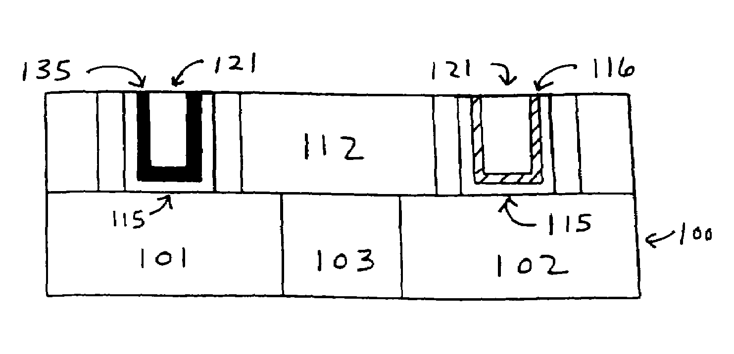
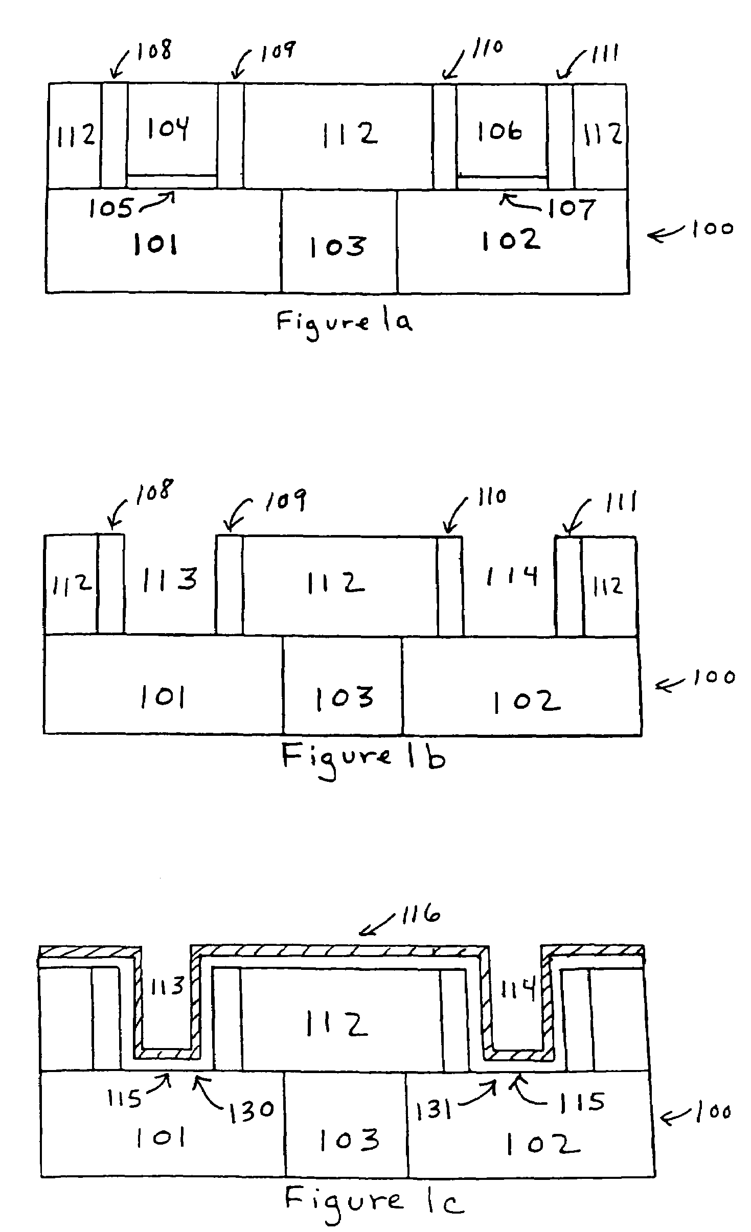
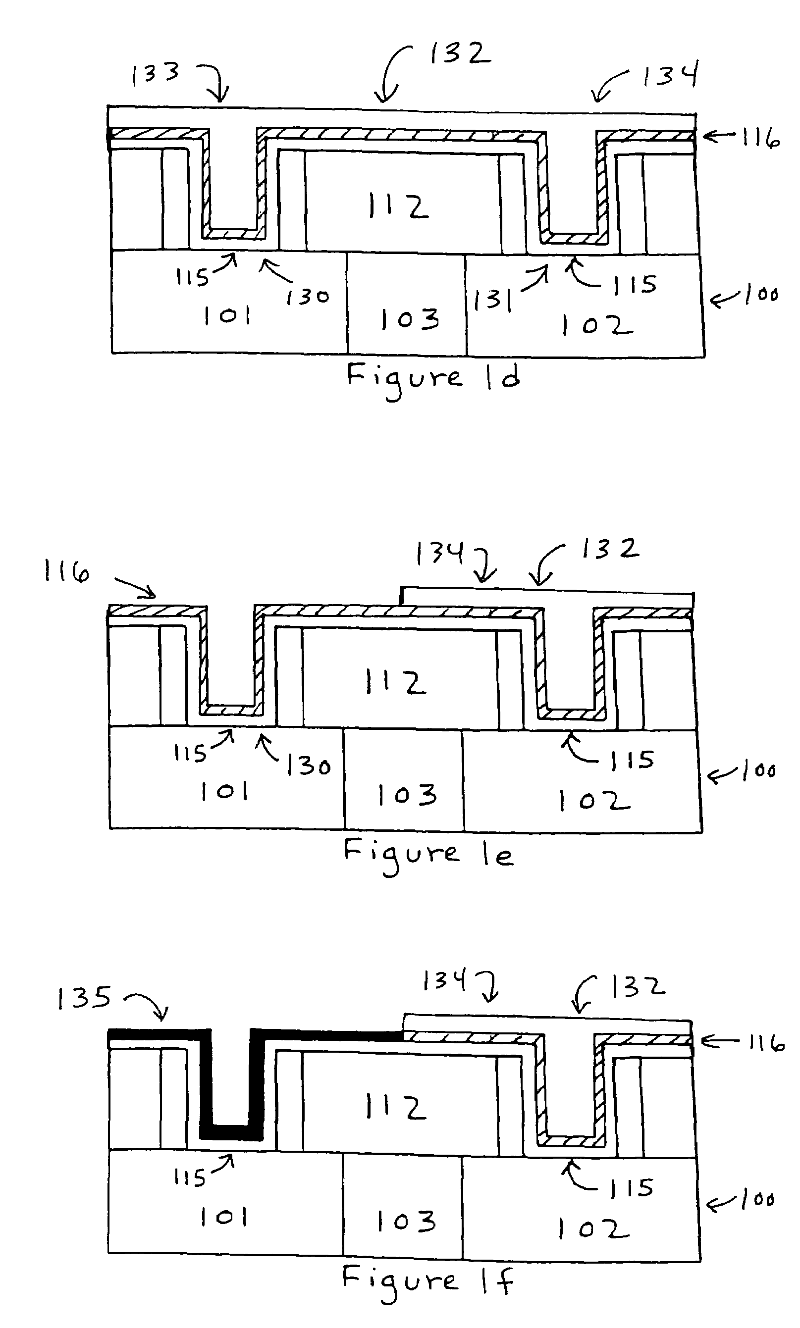
[0011]A method for making a semiconductor device is described. That method comprises forming a first dielectric layer on a substrate, forming a trench within the first dielectric layer, and forming a second dielectric layer on the substrate. The second dielectric layer has a first part that is formed at the bottom of the trench and a second part. A first metal layer with a first workfunction is formed on the first part of the second dielectric layer and on the second part of the second dielectric layer. The first metal layer, where formed on the first part of the second dielectric layer, is then converted into a second metal layer with a second workfunction.

[0012]In the following description, a number of details are set forth to provide a thorough understanding of the present invention. It will be apparent to those skilled in the art, however, that the invention may be practiced in many ways other than those expressly described here. The invention is thus not limited by the specific...


PUM

PropertyMeasurementUnit
temperatureaaaaaaaaaa
workfunctionaaaaaaaaaa

Abstract

A method for making a semiconductor device is described. That method comprises forming a first dielectric layer on a substrate, a trench within the first dielectric layer, and a second dielectric layer on the substrate. The second dielectric layer has a first part that is formed in the trench and a second part. After a first metal layer with a first workfunction is formed on the first and second parts of the second dielectric layer, part of the first metal layer is converted into a second metal layer with a second workfunction.

Description

FIELD OF THE INVENTION[0001]The present invention relates to methods for making semiconductor devices, in particular, semiconductor devices that include metal gate electrodes.BACKGROUND OF THE INVENTION[0002]MOS field-effect transistors with very thin gate dielectrics made from silicon dioxide may experience unacceptable gate leakage currents. Forming the gate dielectric from certain high-k dielectric materials, instead of silicon dioxide, can reduce gate leakage. Because, however, such a dielectric may not be compatible with polysilicon, it may be desirable to use metal gate electrodes in devices that include high-k gate dielectrics.[0003]When making a CMOS device that includes metal gate electrodes, a replacement gate process may be used to form gate electrodes from different metals. In one variant of that process, polysilicon layers are removed to create first and second trenches. Both trenches are filled with a first metal layer. The first metal layer is then removed from the fi...

Claims


Application Information

Patent Timeline
Patent Type & Authority Patents(United States)
IPC IPC(8): H01L21/8238
CPCH01L21/823842
Inventor DOCZY, MARK L.BRASK, JUSTIN K.KAVALIEROS, JACKSHAH, UDAYMETZ, MATTHEW V.DATTA, SUMANNAGISETTY, RAMUNECHAU, ROBERT S.
Owner TAHOE RES LTD
Why Eureka
Try Eureka