Void-free circuit board and semiconductor package having the same

a technology of void-free circuit boards and semiconductors, applied in the direction of printed circuit aspects, sustainable manufacturing/processing, final product manufacturing, etc., can solve the problems of weakened power of supporting the semiconductor chip b>1/b>, and parts in contact with the solder ball b>7/b> may be damaged

Inactive Publication Date: 2008-07-15
SAMSUNG ELECTRO MECHANICS CO LTD
View PDF5 Cites 6 Cited by
  • Summary
  • Abstract
  • Description
  • Claims
  • Application Information

AI Technical Summary

Benefits of technology

[0016]The present invention has been made to solve the foregoing problems of the prior art and therefore an object of certain embodiments of the present invention is to provide a void-free circuit board capable of preventing formation of voids with air captured therein due to non-uniform capillary action during a process of injecting underfill material between a semiconductor chip and a substrate.
[0017]Another object of certain embodiments of the invention is to provide a semiconductor package which prevents formation of voids with air captured therein due to non-uniform capillary action during a process of injecting underfill material between a semiconductor chip and a substrate, thereby preventing a defective product and improving product reliability.

Problems solved by technology

As a result, the power of supporting the semiconductor chip 1 is weakened and portions in contact with the solder balls 7 may be damaged due to stress from vibration.

Method used


Image

  • Void-free circuit board and semiconductor package having the same
  • Void-free circuit board and semiconductor package having the same
  • Void-free circuit board and semiconductor package having the same

Examples


first embodiment

[0054]FIG. 3 is a sectional view illustrating a flip-chip semiconductor package according to the present invention, FIG. 4(a) is a partial plan view illustrating a major part thereof, and FIG. 4(b) is a partial sectional view illustrating the major part thereof.

[0055]As shown in FIGS. 3, 4(a) and 4(b), the flip-chip semiconductor package 100 includes a semiconductor chip 110, a substrate 120, an underfill part 130 and a gap compensation part 140.

[0056]The semiconductor chip 110 is composed of at least one active chip component flip-chip bonded via solder balls 125 onto an upper surface of the substrate 120.

[0057]The substrate 120 has electrode patterns 122 printed or laminated with conductive material such as Cu or Ni according to a pattern designed in advance on an upper surface thereof.

[0058]The electrode pattern 122 has a connection terminal 122a at an end thereof, corresponding to an electrode terminal (not shown) formed on an undersurface of the semiconductor chip 110.

[0059]A s...

second embodiment

[0074]FIG. 5(a) is a partial plan view of a major part of a flip-chip semiconductor package according to the present invention, and FIG. 5(b) is a partial sectional view thereof.

[0075]As shown in FIGS. 5(a) and (b), the gap compensation part 140 in the opening 126 can have a protrusion 142 extended in a predetermined length on the substrate 120 from the inner rim of the protective layer 124 that forms a boundary with the opening 126, to the solder ball 126.

[0076]The protrusion 142 is made of the same material as the protective layer 124 and can be integrally formed as the protective layer 124 is applied. It is preferable that a front end of the protrusion 142 is extended to the vicinity of an outer surface of the solder ball 128 to facilitate the flow of the underfill material via the protrusion 142 to the solder ball 128.

third embodiment

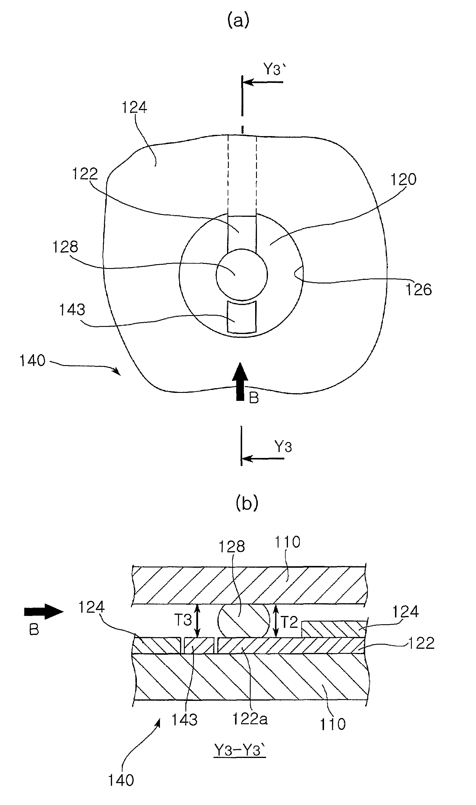
[0077]FIG. 6(a) is a partial plan view illustrating a major part of a flip-chip semiconductor package according to the present invention, and FIG. 6(b) is a partial sectional view thereof.

[0078]As shown in FIGS. 6(a) and (b), the gap compensation part 140 in the opening 126 may have a protrusion 143 separately provided on the substrate 120 without having an end in contact with the electrode pattern 122 nor the other end in contact with the protective layer 124.

[0079]Herein, the protrusion 143 may be made of the same material as the electrode pattern 122 during the process of forming the electrode pattern 122, or alternatively, can be made of the same material as the protective layer 124 during the process of forming the protective layer 124.

[0080]In addition, an encapsulant (not shown) of resin such as epoxy can be formed over the semiconductor chip 110 and the substrate 120 to protect them from the outside environment.


PUM


Abstract

A void-free circuit board and a semiconductor package having the same includes a protective layer covering and protecting an electrode pattern formed on an upper surface of a substrate. The protective layer is applied around a solder ball provided on the electrode pattern except on an immediate vicinity of the solder ball to form an opening. The semiconductor package also includes at least one gap compensation part comprising a protrusion that comes in contact with an underfill material injected to the opening before the electrode pattern. The protrusion has a thickness substantially the same as that of a portion of the electrode pattern exposed in the opening. This prevents voids with air captured therein due to non-uniform capillary action during injection of the underfill material.

Description

CLAIM OF PRIORITY[0001]This application claims the benefit of Korean Patent Application No. 2005-95027 filed on Oct. 10, 2005, in the Korean Intellectual Property Office, the disclosure of which is incorporated herein by reference.BACKGROUND OF THE INVENTION[0002]1. Field of the Invention[0003]The present invention relates to a void-free circuit board and a semiconductor package having the same. More particularly, a void-free circuit board capable of preventing voids with air captured therein due to non-uniform capillary action resulting from an uneven gap formed between a semiconductor chip and a substrate during a process of injecting underfill material into the gap, thereby preventing a defective product and improving product reliability, and a semiconductor package having the same.[0004]2. Description of the Related Art[0005]Recent trend of compact and miniaturized electronic devices has required high-speed, high-function and high-density mounting methods in the packaging techno...

Claims


Application Information

Patent Timeline
Patent Type & Authority Patents(United States)
IPC IPC(8): H01L29/40
CPCH01L21/563H01L23/49838H01L24/28H05K1/111H05K3/3452H01L2924/01023H01L24/81H01L2224/16225H01L2224/73203H01L2224/73204H01L2224/81801H01L2224/83102H01L2224/92125H01L2924/01005H01L2924/01029H01L2924/01033H01L2924/01078H01L2924/01082H01L2924/19041H01L2924/19042H01L2924/19043H01L2924/3025H05K2201/09781H05K2201/0989H05K2201/10674H05K2201/10977H01L2924/01006H01L2924/3512H01L2924/00Y02P70/50
Inventor CHOI, BONG RAK
Owner SAMSUNG ELECTRO MECHANICS CO LTD
Why Eureka
Try Eureka