Method of forming through-silicon vias with stress buffer collars and resulting devices

a technology of throughsilicon vias and buffer collars, which is applied in the direction of semiconductor devices, semiconductor/solid-state device details, electrical apparatus, etc., can solve the problems of significant stress in silicon and copper (or other conductive materials), reducing transistor performance, and reducing yield and reliability failures

Inactive Publication Date: 2008-07-22
INTEL CORP
View PDF12 Cites 365 Cited by
  • Summary
  • Abstract
  • Description
  • Claims
  • Application Information

AI Technical Summary

Problems solved by technology

For example, copper has a CTE of approximately 16.5 ppm / ° C., whereas silicon has a CTE of approximately 2.6 ppm / ° C. This CTE mismatch may result in significant stress in the silicon and copper (or other conductive material) after copper deposition, as well as during any subsequent temperature cycling (e.g., as may occur during solder reflow, during testing, or during use).
The stresses that may result from the above-described CTE mismatch can lead to numerous problems, including thin-film delamination, cracking of the silicon, and reduced transistor performance (any of which may lead to lower yields and reliability failures).

Method used


Image

  • Method of forming through-silicon vias with stress buffer collars and resulting devices
  • Method of forming through-silicon vias with stress buffer collars and resulting devices
  • Method of forming through-silicon vias with stress buffer collars and resulting devices

Examples


Embodiment Construction

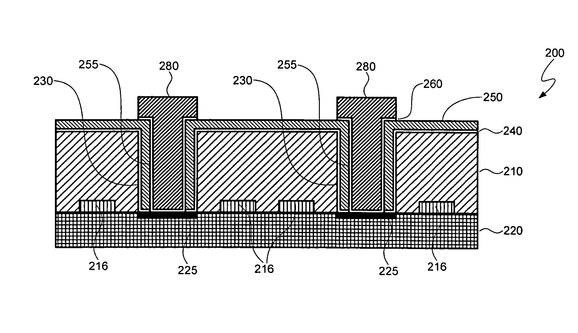
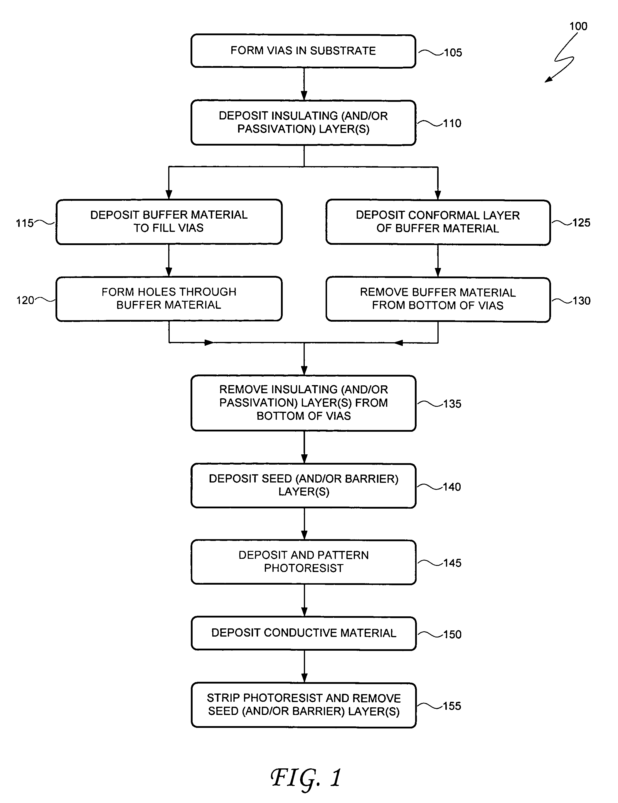
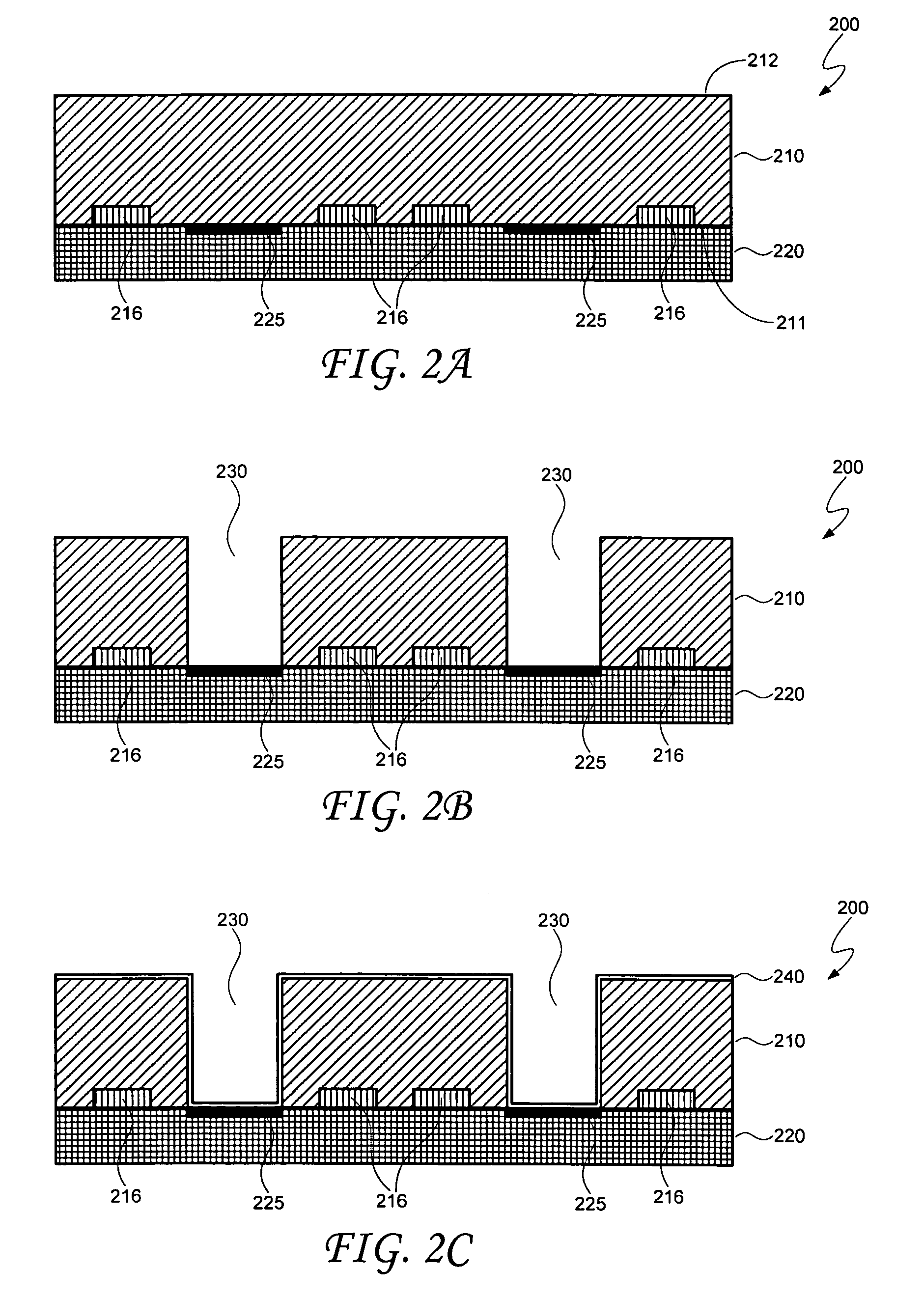
[0009]Turning now to FIG. 1, illustrated is an embodiment of a method 100 of forming a via having a stress buffer collar. Embodiments of the method 100 shown in FIG. 1 are further illustrated in the schematic diagrams of FIGS. 2A through 2L, and reference should be made to these figures as called out in the text below.

[0010]Referring to block 105 in FIG. 1, one or more vias are formed in a substrate. This is illustrated in FIGS. 2A and 2B. Referring first to FIG. 2A, a substrate 200 is shown, this substrate including a base layer 210. In one embodiment, the base layer 210 comprises silicon (Si); however, it should be understood that the substrate may comprise any other suitable material or combination of materials. The substrate's base layer 210 may be viewed as having a “front side”211 and a “back side”212 (the substrate 200 is depicted face down in the figures). It should be understood, however, that the labels “front side” and “back side” are arbitrary and, further, that the vari...


PUM

PropertyMeasurementUnit
thicknessaaaaaaaaaa
thicknessaaaaaaaaaa
thermal expansionaaaaaaaaaa

Abstract

A method of forming a via having a stress buffer collar, wherein the stress buffer collar can absorb stress resulting from a mismatch in the coefficients of thermal expansion of the surrounding materials. Other embodiments are described and claimed.

Description

FIELD OF THE INVENTION[0001]The disclosed embodiments relate generally to the fabrication of integrated circuit devices and, more specifically, to the formation of through-silicon vias with stress buffer collars.BACKGROUND OF THE INVENTION[0002]Vias are routinely used structures in the construction of integrated circuit (IC) devices. By way of example, vias may be used to form electrical connections between various layers of conductors in the interconnect structure of an IC die. By way of further example, vias may also be formed that extend from the backside of an IC die to the active or front side, such vias often referred to as “through-silicon vias.” Through-silicon vias can, for example, be used to form backside interconnects for a pair of bonded wafers, the bonded wafers forming a wafer stack that is ultimately cut into a number of stacked die. In addition, through-silicon vias may also find use in MEMS (Micro-Electromechanical Systems) devices.[0003]Through-silicon vias may be...

Claims


Application Information

Patent Timeline
Patent Type & Authority Patents(United States)
IPC IPC(8): H01L21/4763H01L21/44
CPCH01L21/76898H01L2224/13H01L2924/1461H01L2924/00H01L21/28H01L21/4763
Inventor ARANA, LEONEL R.NATEKAR, DEVENDRANEWMAN, MICHAELGURUMURTHY, CHARAN K.
Owner INTEL CORP
Why Eureka
Try Eureka